Novel stacked thin-film solar cell and manufacturing method thereof (a-Si:H/a-SiGe:H/CIGS or CZTS stacked solar cell and manufacturing method thereof)
A technology of thin-film solar cells and manufacturing methods, applied in sustainable manufacturing/processing, final product manufacturing, circuits, etc., can solve problems such as high absorption coefficient, narrow optical band gap, and not very matching solar spectrum, and achieve high photoelectric conversion efficiency effect
- Summary
- Abstract
- Description
- Claims
- Application Information
AI Technical Summary
Problems solved by technology
Method used
Image
Examples
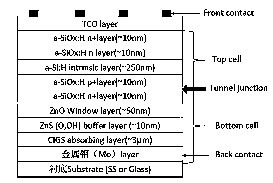
Embodiment 1
[0017] On the glass substrate, a thin layer of Mo with a thickness of ~10nm was deposited by DC magnetron sputtering technology (atmospheric pressure ~1.2-1.5pa, temperature ~400°C);
[0018] Then linearly reduce the gas pressure to ~0.2-0.5Pa, sputter ~1μm thick Mo thin layer;
[0019] Deposit ~3 μm thick CIGS (atomic ratio Cu / (In+Ga)~0.88, Ga / (In+Ga)~0.3) absorber layer;
[0020] By chemical bath deposition (ZnSO 4 (0.16 M), ammonia water (7.5 M), thiourea (0.6 M)) to prepare a ~10 μm thick ZnS buffer layer;
[0021] A dense ZnO film with a thickness of ~50nm was prepared by sputtering;
[0022] Anneal the ZnO thin film at 450°C for 30min;
[0023] Using PECVD process, in SiH 4 ,PH 3 , CO 2 , H 2 Deposit a n-type heavily doped a-SiOx:H transition layer with a thickness of ~10nm under the atmosphere;
[0024] Using PECVD process, in SiH 4 , BF 3 , CO 2 , H 2 Deposit a p-type heavily doped a-SiOx:H back electrode layer with a thickness of ~10nm under the atmospher...
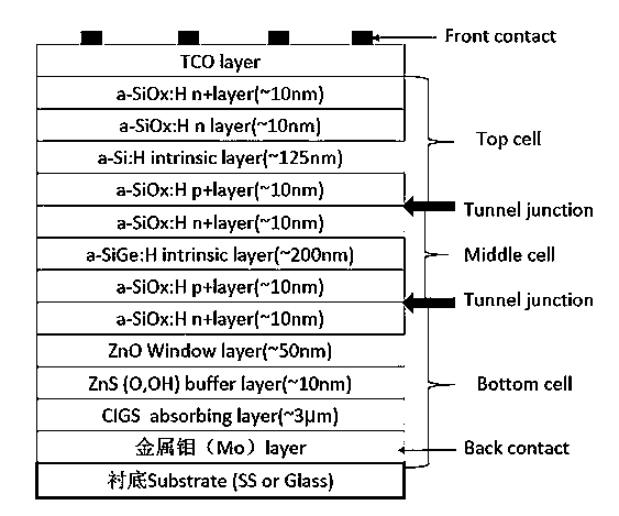
Embodiment 2
[0030] On the glass substrate, a thin Mo layer with a thickness of ~10nm was deposited by DC magnetron sputtering technology (atmospheric pressure ~1.2-1.5pa, temperature ~400℃);
[0031] Then linearly reduce the gas pressure to ~0.2-0.5Pa, sputter ~1μm thick Mo thin layer;
[0032] Deposit ~3 μm thick CIGS (atomic ratio Cu / (In+Ga)~0.88, Ga / (In+Ga)~0.3) absorber layer;
[0033] By chemical bath deposition (ZnSO 4(0.16 M), ammonia water (7.5 M), thiourea (0.6 M)) to prepare a ~10 μm thick ZnS buffer layer;
[0034] A dense ZnO film with a thickness of ~50nm was prepared by sputtering;
[0035] Anneal the ZnO thin film at 450°C for 30min;
[0036] Using PECVD process, in SiH 4 ,PH 3 , CO 2 , H 2 Deposit ~10nm thick n-type heavily doped a-SiOx:H battery transition layer under atmosphere;
[0037] Using PECVD process, in SiH 4 , BF 3 , CO 2 , H 2 Deposit a p-type heavily doped a-SiOx:H battery back electrode layer with a thickness of ~10nm under the atmosphere;
[003...
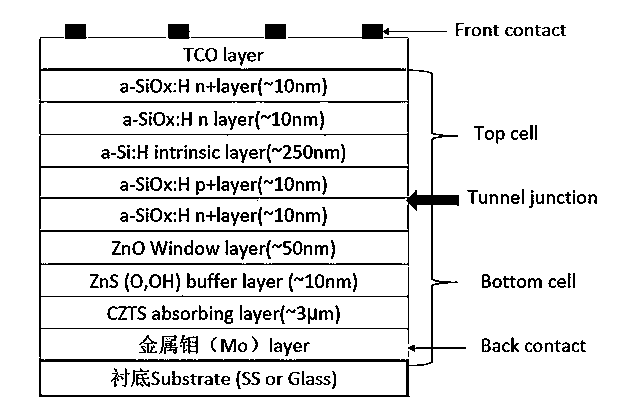
Embodiment 3
[0046] On the glass substrate, a thin Mo layer with a thickness of ~10nm was deposited by DC magnetron sputtering technology (atmospheric pressure ~1.2-1.5pa, temperature ~400℃);
[0047] Then linearly reduce the gas pressure to ~0.2-0.5Pa, sputter ~1μm thick Mo thin layer;
[0048] A CZTS absorber layer with a thickness of ~3 μm was prepared by co-evaporation technique;
[0049] By chemical bath deposition (ZnSO 4 (0.16 M), ammonia water (7.5 M), thiourea (0.6 M)) to prepare a ~10 μm thick ZnS buffer layer;
[0050] A dense ZnO film with a thickness of ~50nm was prepared by sputtering;
[0051] Anneal the ZnO thin film at 450°C for 30min;
[0052] Using PECVD process, in SiH 4 ,PH 3 , CO 2 , H 2 Deposit a n-type heavily doped a-SiOx:H transition layer with a thickness of ~10nm under the atmosphere;
[0053] Using PECVD process, in SiH 4 , BF 3 , CO 2 , H 2 Deposit a p-type heavily doped a-SiOx:H back electrode layer with a thickness of ~10nm under the atmosphere;...
PUM
 Abstract
Description
Claims
Application Information


