Perovskite-based thin film solar cell and preparing method thereof

A thin-film solar cell and perovskite technology, applied in circuits, photovoltaic power generation, electrical components, etc., can solve the problem of low hole mobility, achieve simple manufacturing process, easy operation, and expand the application range

Active Publication Date: 2015-02-25
深圳市华物光能技术有限公司
View PDF7 Cites 26 Cited by
  • Summary
  • Abstract
  • Description
  • Claims
  • Application Information

AI Technical Summary

Problems solved by technology

Among them, the polymer hole transport material has good stability, but the hole mobility is low. If it can be modified to...

Method used


Image

  • Perovskite-based thin film solar cell and preparing method thereof
  • Perovskite-based thin film solar cell and preparing method thereof
  • Perovskite-based thin film solar cell and preparing method thereof

Examples


preparation example Construction

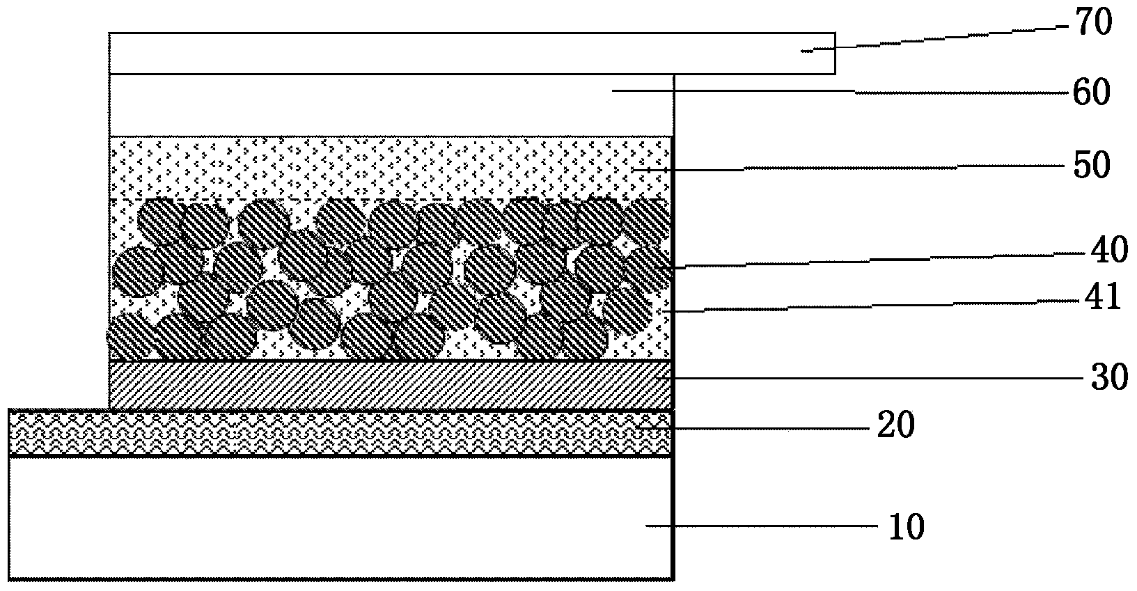
[0043] According to another aspect of the present invention, a method for preparing a perovskite-based thin film solar cell is also provided, including the step of forming a hole transport layer 60 . Wherein, the step of forming the hole transport layer 60 includes: uniformly dispersing the polymer capable of hole transport and graphyne into an organic solvent to form a mixed slurry, and then arranging the mixed slurry on a preformed porous support layer 40 or its capping layer 50; the mixed slurry is dried to form a hole transport layer 60.

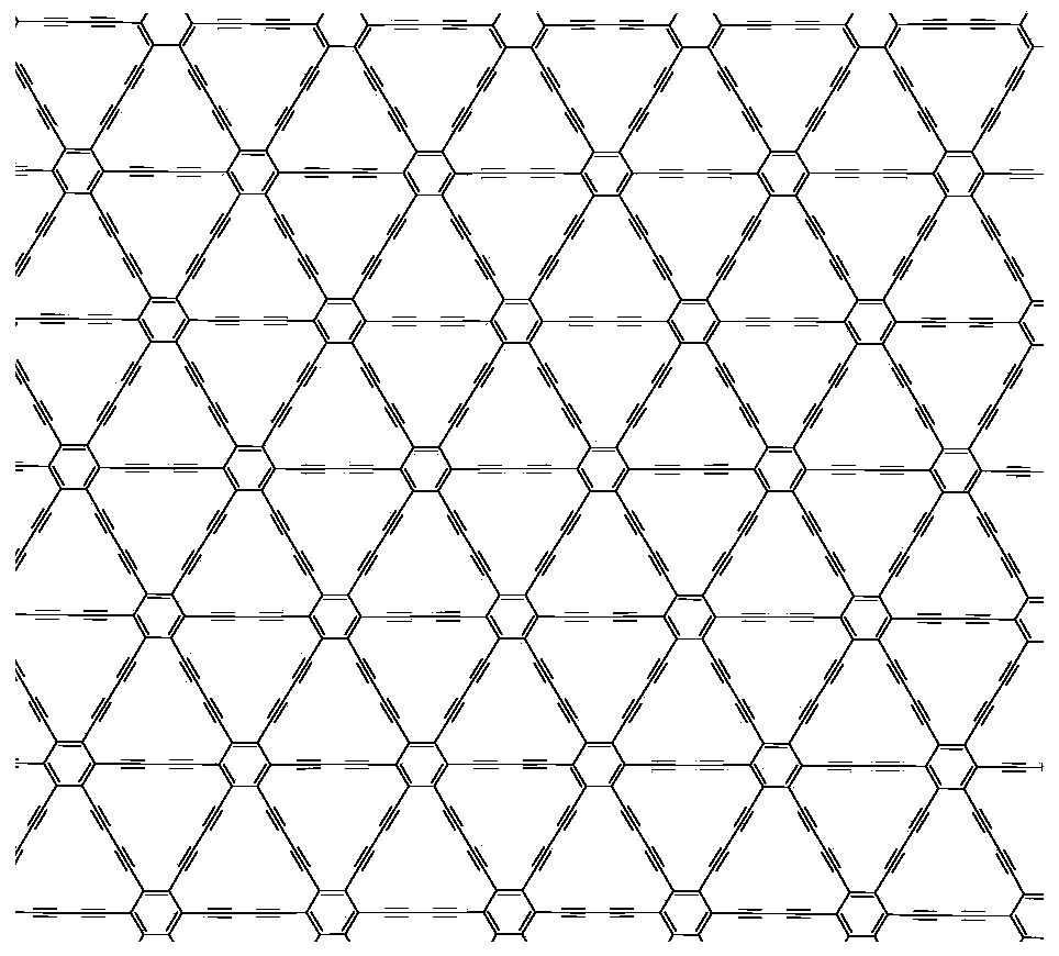
[0044] In actual operation, the graphdiyne is generally dispersed in an organic solvent first, and then the polymer material is added after stirring evenly. After the mixed slurry is formed, the mixed slurry is deposited on the porous support layer 40 by coating or screen printing, and then the slurry is dried to form the hole transport layer 60 on the porous support layer 40 . The organic solvent is selected from one or more of benzene...
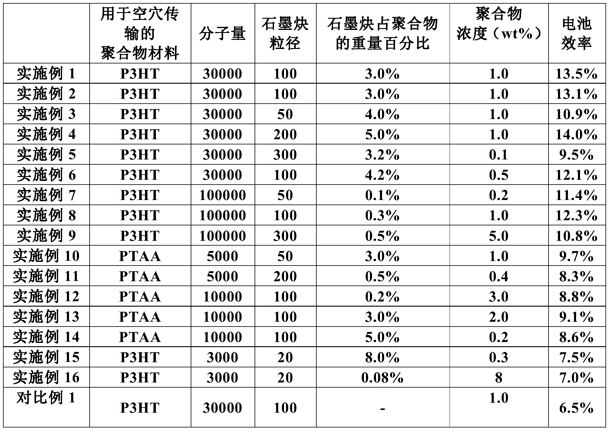
Embodiment 1

[0049] First, a layer of TiO was screen-printed on the FTO glass 2 Thin film layer, after heating at 450° C. for 30 minutes, a dense layer of semiconductor material with a thickness of 50 nm is obtained. Preferably, the dense layer is formed by printing using the screen printing method disclosed in literature (Chin. Phys. Lett., 2006, 23(9), 2606-2608). TiO coating on dense layer by spin coating method 2 The nanoparticle material is dried at room temperature and then sintered at 500°C to obtain a porous scaffold layer structure with a thickness of 100nm.

[0050] Using a two-step method—spin coating followed by dipping: the PbI 2 Dissolved in N,N-dimethylformamide to prepare a spin-coating solution with a concentration of 32% by mass, spin-coat on the porous support layer at a speed of 3000 rpm, and spin-coat for 30 seconds. Spin-coated PbI 2 The porous scaffold layer film was soaked in CH at a concentration of 10 mg / mL 3 NH 3 In the I solution, an organic metal semicond...

Embodiment 2

[0053] First, a layer of TiO was screen-printed on the FTO glass 2 Thin film layer, after heating at 450° C. for 30 minutes, a dense layer of semiconductor material with a thickness of 50 nm is obtained. Preferably, the dense layer is formed by printing using the screen printing method disclosed in literature (Chin. Phys. Lett., 2006, 23(9), 2606-2608). TiO coating on dense layer by spin coating method 2 The nanoparticle material is dried at room temperature and then sintered at 500°C to obtain a porous scaffold layer structure with a thickness of 100nm.

[0054] The organometallic semiconductor light-absorbing material with a perovskite structure is deposited on the porous scaffold layer by a one-step method. The process includes: equimolar amounts of PbI 3 with organic ammonium iodide CH 3 NH 3 I is co-dissolved in N,N-dimethylformamide, prepared as a spin coating solution with a concentration of 40wt%, and the organometallic semiconductor light-absorbing material is fi...


PUM

PropertyMeasurementUnit
Particle sizeaaaaaaaaaa
Thicknessaaaaaaaaaa
Thicknessaaaaaaaaaa

Abstract

The invention discloses a perovskite-based thin film solar cell and a preparing method thereof. The perovskite-based thin film solar cell comprises a hole transfer layer, wherein the hole transfer layer comprises a polymer capable of conducting hole transfer and graphdiyne dispersed in the polymer. In the perovskite-based thin film solar cell, a perovskite material adopted for an absorbing layer generates excitons by absorbing sunlight and separates the excitons into electrons and holes, the electrons are collected through a dense layer which is made from a semiconductor material and guided out to an external circuit through a conductive layer, and the holes are collected through the hole transfer layer and guided out through electrodes. According to the perovskite-based thin film solar cell and the preparing method thereof, the graphdiyne is dispersed in the polymer capable of conducting hole transfer to form a polymer-graphdiyne composite material which serves as the hole transfer layer of the perovskite-based thin film solar cell, and compared with a tradition perovskite-based thin film solar cell only comprising a polymer hole transfer layer, the perovskite-based thin film solar cell has the advantages that the hole transfer ability of the hole transfer layer is improved, and the conversion efficiency of the solar cell is improved.

Description

technical field [0001] The invention relates to the technical field of perovskite-based solar cells, in particular to a perovskite-based thin film solar cell and a preparation method thereof. Background technique [0002] A solar cell is a device that directly converts light energy into electrical energy through the photoelectric effect or photochemical effect, also known as a photovoltaic cell. Its power generation utilizes the photovoltaic effect of specific semiconductor materials. Specifically, the interaction between light and semiconductors generates photogenerated carriers, and the photogenerated electron-hole pairs reach the two poles respectively through the built-in electric field formed inside the semiconductor, generating a potential. When it is connected to an external circuit, it can continuously generate current from a source. This semiconductor optoelectronic device should meet the following two conditions: 1) The energy of the incident light should be great...

Claims


Application Information

Patent Timeline
IPC IPC(8): H01L51/42H01L51/44H01L51/46H01L51/48
CPCH10K85/113H10K30/00H10K30/88Y02E10/549
Inventor 孟庆波李冬梅肖俊彦罗艳红
Owner 深圳市华物光能技术有限公司
Why Eureka
Try Eureka