High temperature pressure sensor and process method thereof

A technology of pressure sensor and processing method, which is applied in the direction of fluid pressure measurement by changing ohmic resistance, can solve the problems of difficult long-term operation of silicon-based sensors, and achieve the effects of eliminating leakage current, improving working temperature, and good thermal stability.

Active Publication Date: 2015-04-22
PEKING UNIV
View PDF5 Cites 15 Cited by
  • Summary
  • Abstract
  • Description
  • Claims
  • Application Information

AI Technical Summary

Problems solved by technology

[0003] The purpose of the present invention is to provide a high-temperature pressure sensor and its processing method to sol

Method used


Image

  • High temperature pressure sensor and process method thereof
  • High temperature pressure sensor and process method thereof
  • High temperature pressure sensor and process method thereof

Examples


Embodiment Construction

[0017] In order to make the above objects, features and advantages of the present invention more obvious and understandable, the present invention will be further described in detail below in conjunction with the accompanying drawings and specific embodiments.

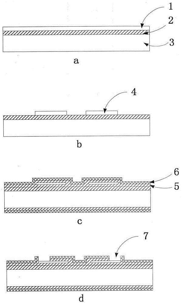
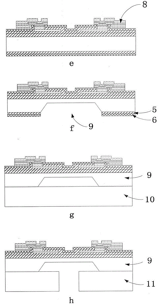
[0018] figure 1 (a)~ figure 1 (h) is a schematic diagram of the main processing technology of the high-temperature pressure sensor processed by the present invention;

[0019] figure 1 (a) shows the double-sided polished SOI single-crystal silicon wafer used for processing the high-temperature pressure sensor of the present invention, the device layer 1 is N (100) single-crystal silicon, and the thickness of the buried oxide layer 2 is The substrate layer 3 has a thickness of 400um.

[0020] Such as figure 1 As shown in (b), perform boron ion implantation and annealing, and etch the device layer of the substrate to form the bridge arm resistance 4 of the Wheatstone bridge. Since increasing the doping concentratio...


PUM


Abstract

The invention discloses a high temperature pressure sensor and a process method thereof, the pressure sensor comprises a silicon-sensitive diaphragm, a pedestal and a TO tube case, wherein a SOI monocrystalline silicon wafer is used as a substrate of the silicon-sensitive diaphragm. A wheatstone bridge is formed by resistance processing and leading wire interconnection in a device layer, and a diaphragm structure which is sensitive to pressure is formed by conducting anisotropy corrosion at a substrate layer. Anodic bonding or silicon-silicon direct bonding or silicon-silicon medium bonding is conducted by the pedestal and the silicon-sensitive diaphragm, wherein the glass sheet or the monocrystalline silicon wafer is used as a substrate of the pedestal. Chip scale package is achieved by using the TO metal tube case for a shell. The high temperature pressure sensor and the process method thereof use a buried oxide layer of the SOI monocrystalline silicon wafer and an illuvial silicon dioxide/silicon nitride passivation layer to wrap and isolate a silicon resistor, and leakage current at high temperature is eliminated. A high temperature ohmic contact electrode structure of multiple layers of silicon dioxide/titanium/ silicon dioxide/ platinum/gold is grown in a spurting mode. Through high temperature resistance bonding and TO packaging technology, the working stability at high temperature is improved. The problem that long term working is difficult to conduct in a high temperature environment by a traditional silicon substrate sensor is solved.

Description

technical field [0001] The invention relates to the field of microelectronic machining, in particular to a high-temperature pressure sensor and a processing method thereof. Background technique [0002] High-temperature resistant sensors manufactured based on microelectronic machining technology are widely used in high-temperature extreme environments such as aerospace and industrial production. One reason why traditional pressure sensors are difficult to work in high temperature environments is that traditional piezoresistive pressure sensors use monocrystalline silicon as a substrate, and P-type diffused resistors are made on N-type silicon substrates, relying on reverse-biased PN junction isolation , when the ambient temperature exceeds 120 ° C, the leakage current of the PN junction will increase, and the isolation will fail; another important factor restricting the maximum operating temperature of the pressure sensor is that the resistivity of the traditional electrode ...

Claims


Application Information

Patent Timeline
IPC IPC(8): G01L9/06
Inventor 刘冠东崔万鹏高成臣郝一龙
Owner PEKING UNIV
Why Eureka
Try Eureka