Manufacturing method of gallium-nitride-based high-electron-mobility transistor of flip-chip structure

A high electron mobility, gallium nitride-based technology, applied in the field of fabrication of gallium nitride-based high electron mobility transistors, can solve the problems of rough material interface, reduce the quality of GaN crystals, etc., achieve good heat dissipation performance, and realize device integration Effect

Inactive Publication Date: 2015-04-22
INST OF SEMICONDUCTORS - CHINESE ACAD OF SCI
View PDF5 Cites 12 Cited by
  • Summary
  • Abstract
  • Description
  • Claims
  • Application Information

AI Technical Summary

Problems solved by technology

At the same time, Ga atoms and Si atoms on the surface of the substrate have a remelting corrosio

Method used


Image

  • Manufacturing method of gallium-nitride-based high-electron-mobility transistor of flip-chip structure
  • Manufacturing method of gallium-nitride-based high-electron-mobility transistor of flip-chip structure

Examples


Example Embodiment

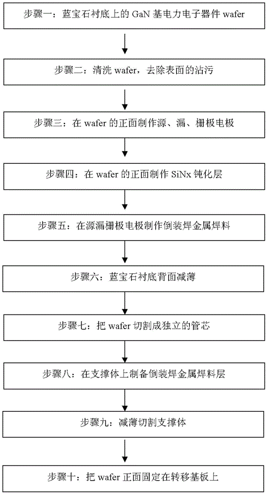
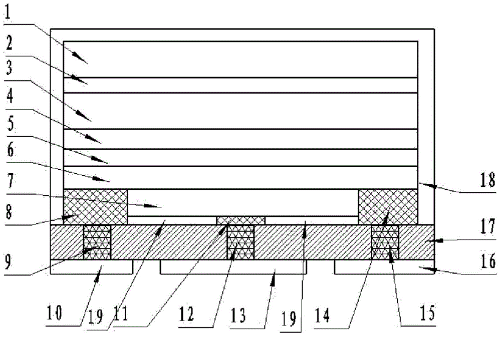
[0022] See figure 1 For reference figure 2 As shown, the present invention provides a method for manufacturing a gallium nitride-based high electron mobility transistor with a flip-chip structure, which includes the following steps:

[0023] Step 1: On the sapphire substrate 1, a low-temperature nucleation layer 2, a gallium nitride high-resistance layer 3, a high-mobility gallium nitride layer 4, an aluminum nitride insertion layer 5, an aluminum gallium nitride barrier layer 6 and The gallium nitride cap layer 7 forms an epitaxial wafer. The material of the low-temperature nucleation layer 2 is gallium nitride, aluminum nitride or aluminum gallium nitride, and the thickness is 20-100 nm. The gallium nitride high resistance layer 3 The thickness of the high-mobility gallium nitride layer 4 is 500-5000nm, the thickness of the high-mobility gallium nitride layer 4 is 10-300nm, the thickness of the aluminum nitride insertion layer 5 is 0-5nm, and the aluminum gallium nitride barri...


PUM

PropertyMeasurementUnit
Thicknessaaaaaaaaaa
Thicknessaaaaaaaaaa
Thicknessaaaaaaaaaa

Abstract

The invention provides a manufacturing method of a gallium-nitride-based high-electron-mobility transistor of a flip-chip structure. The manufacturing method comprises the steps that a low-temperature nucleating layer, a gallium nitride high-resistance layer, a high-mobility gallium nitride layer, an aluminum nitride insertion layer, an aluminum-gallium-nitrogen barrier layer and a gallium nitride capping layer are sequentially grown on a sapphire substrate in an epitaxial mode to form an epitaxial wafer; soaking and washing are conducted; a metal layer is manufactured on a mesa and the gallium nitride capping layer; two windows are manufactured, insulating Si3N4 passivation films are manufactured in the windows, and a Schottky contact electrode as a grid electrode is formed between the two windows; the sapphire substrate is thinned; a flip-chip metal welding flux layer corresponding to an ohmic contact electrode of a source electrode and a flip-chip metal welding flux layer corresponding to an ohmic contact electrode of a drain electrode are manufactured; an electrode lead of the source electrode, an electrode lead of the drain electrode and an electrode lead of the grid electrode are manufactured; a tube core is welded to a supporting body in a flip-chip mode; a Si3N4 protective layer is formed on the surface of the tube core in a vapor deposition mode, and then manufacturing is completed.

Description

Technical field [0001] The invention relates to the field of semiconductor technology, in particular to a manufacturing method of a gallium nitride-based high electron mobility transistor epitaxially grown on a sapphire substrate. The method adopts a flip-chip welding method to fix a gallium nitride-based high electron mobility transistor epitaxially on a sapphire substrate to an insulating substrate with good thermal conductivity such as silicon and aluminum nitride ceramics. Background technique [0002] The main device types of microwave transistors are homojunction bipolar transistor (BJT), heterojunction bipolar transistor (HBT), metal semiconductor field effect transistor (MESFET), metal oxide semiconductor field effect transistor (MOSFET) and high Electron mobility transistor (HEMT) etc. [0003] The forbidden band width of GaN material is large (Eg=3.4eV), and the critical breakdown field strength (3.3MV / cm) is relatively large. The electronic device produced has the chara...

Claims


Application Information

Patent Timeline
IPC IPC(8): H01L21/335
CPCH01L29/66431
Inventor 纪攀峰谢海忠梁萌马平张韵王军喜李晋闽
Owner INST OF SEMICONDUCTORS - CHINESE ACAD OF SCI
Why Eureka
Try Eureka