Electric field controlled graphene/gallium arsenide solar cell and preparation method thereof

A solar cell and electric field regulation technology, applied in the field of solar cells, can solve problems such as poor stability and graphene doping, and achieve the effects of high conversion efficiency, simple process, and easy promotion.

Active Publication Date: 2015-04-29
ZHEJIANG UNIV
View PDF2 Cites 5 Cited by
  • Summary
  • Abstract
  • Description
  • Claims
  • Application Information

AI Technical Summary

Problems solved by technology

Studies in recent years have found that the graphene / semiconductor heterojunction structure is an ideal solar cell structure, but the photoelectric conversion efficiency currently obtained is still significantly lower than the mainstream silicon solar cell efficiency in the market, and one of the important limiting factors is graphite. doping of ene
Graphene can be doped chemically, but it is less stable

Method used


Image

  • Electric field controlled graphene/gallium arsenide solar cell and preparation method thereof
  • Electric field controlled graphene/gallium arsenide solar cell and preparation method thereof

Examples


Embodiment 1

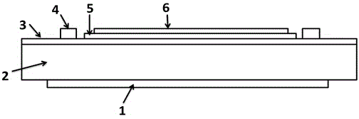
[0027] 1) Electron beam evaporation is used to deposit chromium, nickel and gold composite electrodes on one side of the n-type gallium arsenide wafer;

[0028] 2) Immerse the obtained sample in NaOH aqueous solution with a mass concentration of 10% for surface cleaning, take it out after 30 minutes and dry it;

[0029] 3) transfer the single-layer graphene to the other side of the gallium arsenide sheet after 2) processing;

[0030] 4) Deposit silver electrodes on the graphene layer by thermal evaporation process, and reserve the area for growing insulating dielectric layer;

[0031] 5) Deposit HfO by magnetron sputtering on the area reserved between the silver electrodes on the graphene layer 2 Thin film with a thickness of 5nm;

[0032] 6) In HfO 2 20nm gold is deposited on the film as the gate.

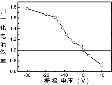
[0033] The effect of the adjusted electric field obtained on the normalized conversion efficiency of graphene / GaAs solar cells is as follows: figure 2 As shown, it can be se...

Embodiment 2

[0035] 1) Deposit titanium, palladium and silver composite electrodes on one side of the p-type gallium arsenide wafer by electron beam evaporation;

[0036] 2) Immerse the obtained sample in HCl aqueous solution with a mass concentration of 10% for surface cleaning, take it out after 5s and dry it;

[0037] 3) Transfer bilayer graphene to 2) the other side of the processed gallium arsenide sheet;

[0038] 4) Deposit the ITO electrode on the graphene layer by using the magnetron sputtering process, and reserve the area for growing the insulating dielectric layer;

[0039] 5) TiO is deposited by magnetron sputtering on the reserved area between the ITO electrodes on the graphene layer 2 Thin film with a thickness of 0.4nm;

[0040] 6) In TiO 2 10nm AZO is deposited on the film as the gate.

Embodiment 3

[0042] 1) Deposit the ITO electrode on one side of the p-type gallium arsenide wafer by magnetron sputtering;

[0043] 2) Immerse the obtained sample in HNO with a mass concentration of 20% 3 Wash the surface in aqueous solution for 5 minutes, take it out and dry it;

[0044] 3) transfer 10 layers of graphene to 2) the other side of the processed gallium arsenide sheet;

[0045] 4) Evaporate gold and palladium composite electrodes on the graphene layer, and reserve the area for growing the insulating dielectric layer;

[0046] 5) Prepare SiN by chemical vapor deposition process on the reserved area of ​​graphene layer x Thin film with a thickness of 100nm;

[0047] 6) In SiN x 80nm FTO is deposited on the film as the gate.


PUM


Abstract

The invention relates to an electric field controlled graphene / gallium arsenide solar cell and a preparation method thereof. The electric field controlled graphene / gallium arsenide solar cell is provided with a back electrode, a gallium arsenide layer, a graphene layer, an insulating medium layer and a grid electrode from bottom to top sequentially; the electric field controlled graphene / gallium arsenide solar cell is further provided with front electrodes, and the front electrodes are arranged on the graphene layer. The preparation method of the electric field controlled graphene / gallium arsenide solar cell comprises steps as follows: the back electrode is manufactured on one side of a gallium arsenide piece; graphene is transferred to the other side of the gallium arsenide piece after the gallium arsenide piece is cleaned; the front electrodes are manufactured on the graphene; the insulating medium layer is manufactured on the graphene; finally, the grid electrode is manufactured on the insulating medium layer, and the solar cell is obtained. According to the electric field controlled graphene / gallium arsenide solar cell, the graphene doping state can be controlled through an external electric field, and the photoelectric converting efficiency of the graphene / gallium arsenide solar cell can be further improved.

Description

technical field [0001] The invention relates to a solar cell and a manufacturing method thereof, in particular to a graphene / gallium arsenide solar cell regulated by an electric field and a preparation method thereof, belonging to the technical field of solar cells. Background technique [0002] As a kind of renewable green energy, solar cells are playing a key role in the sustainable development of human beings. In Germany, where photovoltaic power generation was developed earlier, more than 50% of its power generation comes from photovoltaic power generation. In 2013, China's newly installed photovoltaic capacity also reached 12GW, an increase of more than 200% compared with 2012. Among all photovoltaic power generation technologies, silicon-based solar cells, especially crystalline silicon solar cells, account for about 90% of the market. The purification of silicon materials, the complex process of silicon solar cells and the resulting environmental pollution have also ...

Claims


Application Information

Patent Timeline
Patent Type & Authority Applications(China)
IPC IPC(8): H01L31/0352H01L31/18
CPCH01L31/0328H01L31/0352H01L31/1804H01L31/184Y02E10/544Y02E10/547Y02P70/50
Inventor 林时胜李晓强陈红胜骆季奎李尔平王朋章盛娇徐志娟
Owner ZHEJIANG UNIV
Why Eureka
Try Eureka