Mesoscopic perovskite photovoltaic cell with tin-oxide electron-transporting layer and preparation method thereof
A technology of electron transport layer and photovoltaic cell, which is applied in the direction of photovoltaic power generation, circuits, electrical components, etc., can solve the problems of complex preparation process and high cost of electron transport layer, achieve good photoelectric conversion efficiency and stable performance, reduce production cost, improve Effects of performance and photostability
- Summary
- Abstract
- Description
- Claims
- Application Information
AI Technical Summary
Problems solved by technology
Method used
Image
Examples
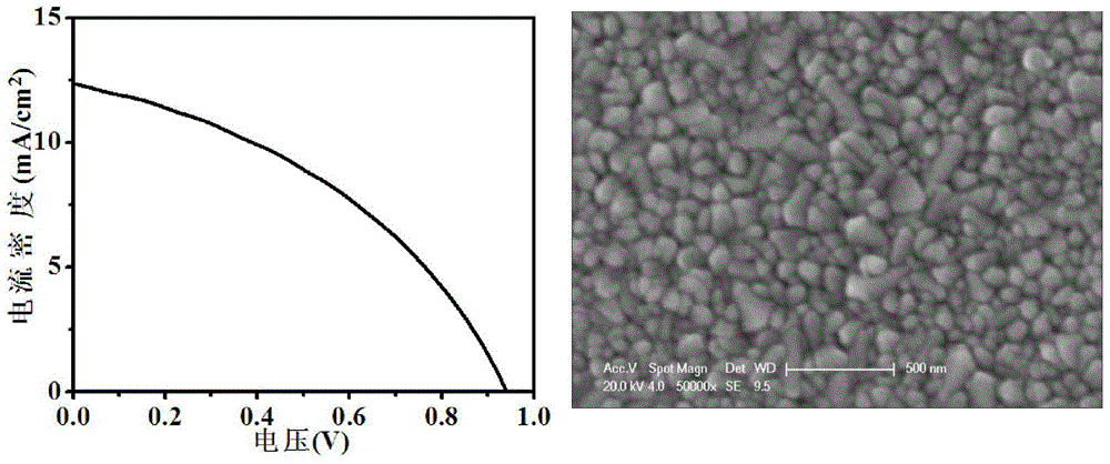
Embodiment 1
[0045] 1) Wash. In the test, the FTO conductive glass substrate should be cleaned and dried first. Clean the FTO conductive glass of appropriate size with detergent first, and then rinse it with deionized water. Then use deionized water, acetone, ethanol to clean ultrasonically, and finally blow dry with nitrogen for later use.
[0046] 2) Perovskite CH 3 NH 3 PB 3 Absorbing layer preparation. Configuration of perovskite solution: 1M PbCl 2 Dissolve in dimethylformamide and stir at 60°C for 24 hours. Then use the homogenizer to mix the PbCl 2 The solution was spin-coated on the FTO conductive glass substrate, and then annealed at 70°C for 30 minutes. Spin coated with PbCl 2 The sample was placed in 10 mg / L CH 3 NH 3 Immerse in isopropanol solution for 10 minutes; finally rinse the sample with isopropanol, blow dry with nitrogen, and anneal at 70°C for 30 minutes.
[0047] 3) Preparation of hole transport layer. perovskite CH with a homogenizer 3 NH 3 PB 3 A lay...
Embodiment 2
[0051] 1) Conductive substrate cleaning. With embodiment 1.
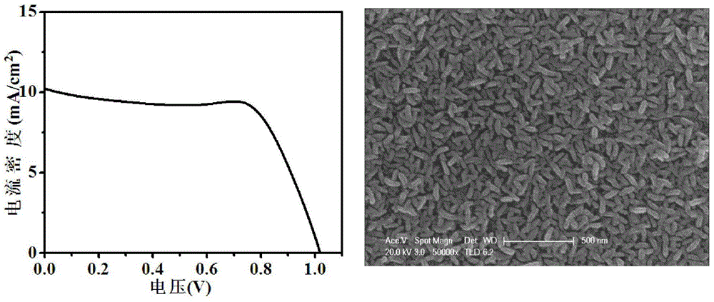
[0052] 2) Electron transport layer preparation. Configuration of hydrothermal solution: Add 0.025Mol / L tin oxalate and 0.025Mol / L hexamethylenetetraammonia into a jar, the solvent is deionized water, stir for 30min; put the cleaned transparent conductive substrate into the step In the prepared solution; put the solution in a 95°C incubator for 3 hours, take it out after naturally cooling to room temperature in the incubator, and deionize the SnO 2 The sediment on the surface of the film was rinsed and dried with nitrogen to obtain SnO 2 dense layer of nanorods, such as image 3 (right) described.
[0053] 3) Perovskite CH 3 NH 3 PB 3 Absorbing layer preparation. With embodiment 1.
[0054] 4) Preparation of hole transport layer. With embodiment 1.
[0055] 5) Electrode preparation. With embodiment 1.
[0056] 6) Test, same as Example 1. The obtained photoelectric conversion efficiency parameters are, o...
Embodiment 3
[0058] 1) Conductive substrate cleaning. With embodiment 1.
[0059] 2) Double-layer nanorod mesoporous SnO 2 Electron transport layer preparation. The configuration of the hydrothermal solution: the same as in Example 2; put the cleaned transparent conductive substrate into the solution prepared in the step; put the solution in a 75°C incubator for 6 hours, and cool it to room temperature naturally in the incubator Take out, deionize the SnO with deionized water 2 The sediment on the surface of the film was washed and dried with nitrogen to obtain SnO 2 Nanorod mesoporous layers, such as Figure 4 (right) described.
[0060] 3) Perovskite CH 3 NH 3 PB 3 Absorbing layer preparation. With embodiment 1.
[0061] 4) Preparation of hole transport layer. With embodiment 1.
[0062] 5) Electrode preparation. With embodiment 1.
[0063] 6) Test, same as Example 1. The obtained photoelectric conversion efficiency parameters are, open circuit voltage 1.06V, short circuit...
PUM
| Property | Measurement | Unit |
|---|---|---|
| Short circuit current density | aaaaa | aaaaa |
Abstract
Description
Claims
Application Information


