A kind of preparation 3c-sic nano disk, preparation method

A nanodisk and nanoparticle technology, applied in nanocarbon, nanotechnology, nanotechnology, etc., can solve the problems of difficult control of luminescence of 3C-SiC nanoparticles, high price of 3C-SiC multi-chips, difficulties in preparation and purchase, and achieve The effect of short preparation cycle, short preparation time and uniform size

Inactive Publication Date: 2017-07-14
BEIJING UNIV OF TECH
View PDF5 Cites 0 Cited by
  • Summary
  • Abstract
  • Description
  • Claims
  • Application Information

AI Technical Summary

Problems solved by technology

However, the preparation process of this method is complicated, and the obtained SiC particles are often larger than 20nm in size.
In addition, 3C-SiC multi-chip is not only expensive, but also difficult to prepare and purchase
[0005] Due to its small size, the structure and properties of nanoparticles are quite complex, and its surface state and defect state have a great influence on its luminescence properties, which makes it difficult to control the luminescence of 3C-SiC nanoparticles. there will be great difficulties
At present, there is no report on the preparation of SiC nanomaterials by hot wire CVD, and there is no technical method to prepare 3C-SiC nanoparticles with a height below 5nm and uniform size.

Method used


Image

  • A kind of preparation 3c-sic nano disk, preparation method
  • A kind of preparation 3c-sic nano disk, preparation method
  • A kind of preparation 3c-sic nano disk, preparation method

Examples


Embodiment 1

[0030] Embodiment 1: The CVD furnace used in the present invention is a hot wire-CVD furnace.

[0031] (1) Silicon wafers were ultrasonically cleaned with methanol, acetone and isopropanone for 15 minutes, N 2 blow dry. Evaporate 10nm Al sequentially by E-Beam Evaporation 2 o 3 , 0.8nm Fe.

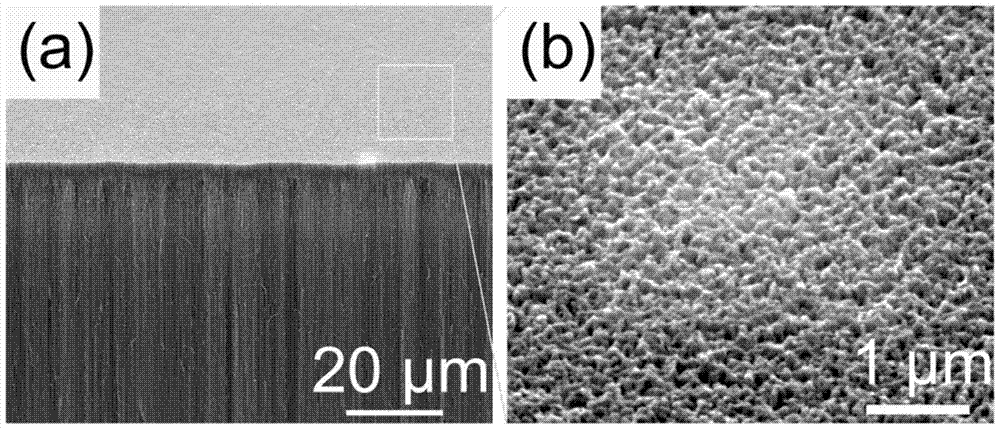
[0032] (2) At a furnace temperature of 725°C, the gas flow rates are H 2 :200sccm, C 2 h 2 : 1.8 sccm, H through deionized water 2 Under the conditions of 200 sccm, total air pressure of 25.5Torr, single tungsten wire, and 35W power, place the silicon chip made in (1) 0.5cm in front of the tungsten wire, and set the power of the tungsten wire to 0 after 30s of reaction , the total air pressure was adjusted to 6.4 Torr, and the vertical array growth of single-walled carbon nanotubes was completed after 15 minutes of reaction.

[0033](3) 10nm Si was evaporated on the vertical array of single-walled carbon nanotubes obtained in (2) by an electron beam evaporation system (E-beam Evapo...

Embodiment 2

[0036] Embodiment 2: The CVD furnace used in the present invention is a hot wire-CVD furnace.

[0037] (1) Silicon wafers were ultrasonically cleaned with methanol, acetone and isopropanone for 15 minutes, N 2 blow dry. Evaporate 10nm Al sequentially by E-Beam Evaporation 2 o 3 , 0.8nm Fe.

[0038] (2) At a furnace temperature of 750°C, the gas flow rates are H 2 :200sccm, C 2 h 2 : 2 sccm, H through deionized water 2 Under the conditions of 200sccm, air pressure of 25Torr, single tungsten wire, and 32W power, place the silicon wafer made in (1) 0.5cm in front of the tungsten wire, and set the power of the tungsten wire to 0 after reacting for 30s. It is adjusted to 6.4 Torr, and the vertical array growth of single-walled carbon nanotubes is completed after 15 minutes of reaction.

[0039] (3) The vertical array of single-walled carbon nanotubes obtained in (2) was vapor-deposited with 5nm Si by E-beam Evaporation.

[0040] (4) At a furnace temperature of 850°C, the g...

Embodiment 3

[0043] Embodiment 3: The CVD furnace used in the present invention is a hot wire-CVD furnace.

[0044] (1) Silicon wafers were ultrasonically cleaned with methanol, acetone and isopropanone for 15 minutes, N 2 blow dry. Evaporate 10nm Al sequentially by E-Beam Evaporation 2 o 3 , 0.8nm Fe.

[0045] (2) At a furnace temperature of 800°C, the gas flow rates are H 2 :190sccm, C 2 h 2 : 2.2 sccm, H through deionized water 2 Under the conditions of 200sccm, total air pressure of 25Torr, single tungsten wire, and 30W power, place the silicon wafer made in (1) 0.5cm in front of the tungsten wire, and set the power of the tungsten wire to 0 after 30s of reaction. The total air pressure was adjusted to 6.4 Torr, and the vertical array growth of single-walled carbon nanotubes was completed after 15 minutes of reaction.

[0046] (3) 3nm Si was evaporated on the vertical array of single-walled carbon nanotubes obtained in (2) by an electron beam evaporation system (E-beam Evaporat...


PUM

PropertyMeasurementUnit
diameteraaaaaaaaaa
heightaaaaaaaaaa
diameteraaaaaaaaaa

Abstract

The invention discloses a 3C-SiC nanometer disc and a preparation method thereof, and belongs to the field of silicon carbide carbon nano-material preparation. The 3C-SiC nanometer particle is in a shape of a disc and has the diameter of 5-30nm and height of 1.5-5nm. A single-walled carbon nanotube array vertically grows on a silicon chip, a Si layer is formed on the top layer of the vertical single-walled carbon nanotube array by evaporation, and the 3C-SiC nanometer disc is prepared on the top layer of the single-walled carbon nanotube array and then is separated. The preparation method has the advantages of simple processes, uniform sample and high crystallization quality.

Description

technical field [0001] The invention belongs to the field of preparing silicon carbide carbon nanometer materials, and in particular relates to a method for preparing 3C-SiC nanodisks with different diameters and heights. Background technique [0002] Silicon carbide (SiC) is one of the core materials of third-generation semiconductors, and it has many advantages compared with the first element semiconductor material (Si) and the second compound semiconductor materials GaAs, GaP and InP. Silicon carbide not only has a large bandgap width (the bandgap widths of 3C, 4H, and 6H types of silicon carbide at room temperature are 2.34, 3.22, and 2.86eV, respectively), but also has a high critical breakdown electric field, high thermal conductivity, and high load. Drift speed and other characteristics of the carrier have great application prospects in high temperature, high frequency, high power, optoelectronics and radiation resistance. Replacing silicon with silicon carbide to pr...

Claims


Application Information

Patent Timeline
Patent Type & Authority Patents(China)
IPC IPC(8): C23C16/32C01B32/16C01B32/984B82Y30/00B82Y40/00
CPCB82Y30/00B82Y40/00C23C14/14C23C16/26C23C16/325
Inventor 郭霞范修军李冲董建刘白刘巧莉
Owner BEIJING UNIV OF TECH
Why Eureka
Try Eureka