Self supporting three dimension device and preparation method thereof

A self-supporting and device technology, applied in semiconductor/solid-state device manufacturing, electrical components, circuits, etc., can solve the problems that micro-nano devices cannot be popularized and applied, and achieve the effects of low cost, good controllability and flexible process

Active Publication Date: 2015-05-06
INST OF PHYSICS - CHINESE ACAD OF SCI
View PDF3 Cites 6 Cited by
  • Summary
  • Abstract
  • Description
  • Claims
  • Application Information

AI Technical Summary

Problems solved by technology

[0003] However, the micro-nano devices with three-dimensional structures obtained by the above-mentioned preparation process all use large-area metal thin films as carriers, and all three-dimensional micro-nano devices are connected to the parent metal film, which requires that each three-dimensional micro-nano devices are insulated from each other. Or require that some parts of each micro-nano device cannot be short-circuited by metals and other fields, which cannot be popularized and applied

Method used


Image

  • Self supporting three dimension device and preparation method thereof
  • Self supporting three dimension device and preparation method thereof
  • Self supporting three dimension device and preparation method thereof

Examples


Embodiment 1

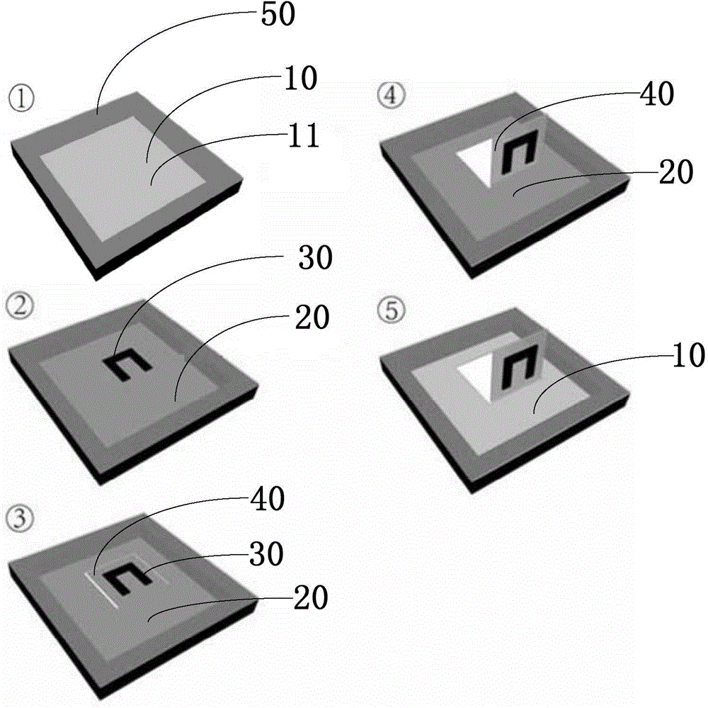
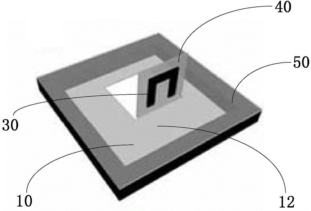
[0048] according to figure 1 The process shown in produces insulating self-supporting 3D devices with metal patterns on the surface.

[0049] Step 1: Deposit metal chromium with a thickness of 3 nm as a conductive layer on a silicon nitride window with a thickness of 50 nm (provided by Shanghai Nateng Instrument Co., Ltd.).

[0050] Step 2: Spin-coat electron beam photoresist PMMA on the conductive layer obtained in step 1 at a speed of 4000r / min, then place the silicon nitride window spin-coated with photoresist on a hot plate at 180°C for 1 minute to make it The solvent evaporates.

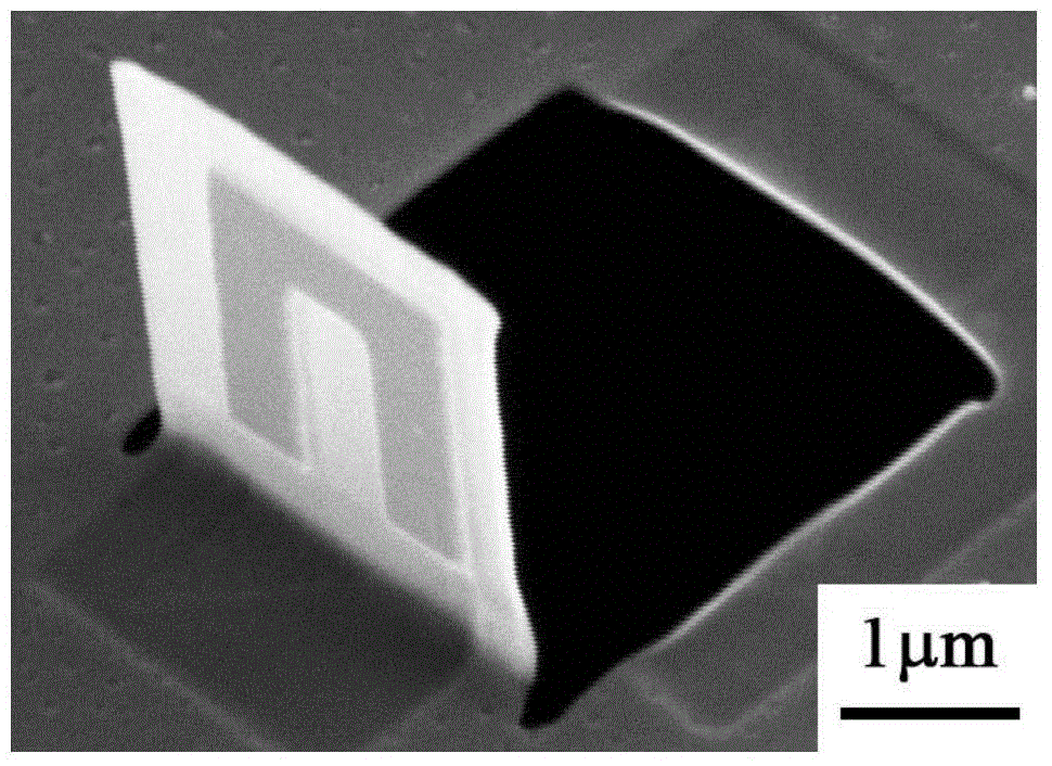
[0051] Step 3: Exposing and developing the sample obtained in step 2) by using an electron beam exposure process to obtain a photoresist pattern with a "U" structure with a side length of 1.7 μm and a line width of 0.5 μm.

[0052] Step 4: Evaporating a gold layer with a thickness of 50 nm on the sample obtained in step 3) by using an electron beam evaporation process.

[0053] Step 5: Soak t...

Embodiment 2

[0058] Step 1: Spin-coat a layer of UV photoresist S1813 on a self-supporting silicon oxide film (provided by Shanghai Nateng Instrument Co., Ltd.) with a thickness of 100nm, and the rotating speed during spin coating is 4000r / min. The self-supporting silicon oxide film of S1813 was baked on a hot plate at 115°C for 2 minutes to evaporate the solvent.

[0059] Step 2: Exposing and developing the sample obtained in Step 1 by using an ultraviolet exposure process to obtain an isosceles right triangle photoresist pattern with a hypotenuse length of 4 μm.

[0060] Step 3: Evaporate a silver film with a thickness of 50 nm on the sample obtained in step 2 by using an electron beam evaporation process.

[0061] Step 4: Soak the sample obtained in step 3 in acetone for 1 hour, gently blow off the silver film on the surface of the sample with a straw, remove the sample and dry it with nitrogen to obtain a metal pattern on the self-supporting silicon oxide film.

[0062] Step 5: On the...


PUM


Abstract

The invention discloses a self supporting three dimension device and a preparation method thereof. The preparation method of the self supporting three dimension device includes: S1, providing a self supporting insulation dielectric film with a basically flat upper surface; S2, generating a conducting layer and at least one device unit with a preset pattern on the upper surface of the self supporting insulation dielectric film so as to generate a composite layer structure; S3, cutting the composite layer structure so as to obtain at least one suspension portion locally connected with the composite layer structure, wherein each suspension portion is provided with each corresponding device unit; S4, using an ion beam to irradiate the at least one suspension portion so as to deform the conducting layer, and thereby driving each suspension portion to bend around a portion of each suspension portion, connected with the composite layer structure, towards the direction far away from the self supporting insulation dielectric film; S5, removing at least a portion of the conducting layer so as to obtain the self supporting three dimension device. The preparation method of the self supporting three dimension device can prepare a three dimensional structure and micron and nanometer devices which are insulated from one another on the self supporting insulation dielectric film, and has the advantages of being good in controllability, low in cost, and capable of preparing the self supporting three dimension device large in area.

Description

technical field [0001] The invention relates to the technical field of three-dimensional micro-nano devices, in particular to a self-supporting three-dimensional device and a preparation method thereof. Background technique [0002] With the development of microelectronics technology, the difficulty of device miniaturization is gradually increasing. The structure of three-dimensional devices has undoubtedly become an important way to increase the integration density of devices. Therefore, finding a method for manufacturing three-dimensional controllable spatial micro-nanostructures has attracted more and more attention. At present, some people use ion beam irradiation to control the deformation of the film to prepare a three-dimensional structure. It uses a focused ion beam to etch a cantilever structure on a self-supporting silver film, and then uses ion beam irradiation to deform the silver cantilever. Three-dimensional metallic structures that can be freely oriented in s...

Claims


Application Information

Patent Timeline
Patent Type & Authority Applications(China)
IPC IPC(8): H01L21/48H01L21/50
Inventor 刘哲李俊杰崔阿娟李无瑕顾长志
Owner INST OF PHYSICS - CHINESE ACAD OF SCI
Why Eureka
Try Eureka