Semiconductor device and manufacturing method thereof

A manufacturing method and semiconductor technology, applied in the direction of semiconductor devices, semiconductor/solid-state device manufacturing, semiconductor/solid-state device components, etc., can solve the problem of increased output power of gallium nitride semiconductor devices, uneven temperature distribution, increased process difficulty, etc. question

Active Publication Date: 2015-05-13
GPOWER SEMICON
View PDF2 Cites 12 Cited by
  • Summary
  • Abstract
  • Description
  • Claims
  • Application Information

AI Technical Summary

Problems solved by technology

[0003] See figure 1 , figure 1 Shows a schematic top view of a gallium nitride semiconductor device in the prior art, the gallium nitride semiconductor device shown includes an active region a and a passive region b, the active region a is in a closed form, and the region outside the active region a It is the passive region b, the source 11, the drain 12 and the gate 13 in the active region a are repeatedly arranged in the width direction of the device to form an overall finger-like structure, the entire semiconductor device is rectangular, and the drain 14 is located in the non-active region. The drain interconnection metal 14 in the source region is connected together, the gate 13 is connected together through the gate interconnection metal 131, and the signal from the outside is received through the lead pad 15, but because the power density of the GaN semiconductor device is very high , so its heat density is also very high, resulting in very large heat generated by GaN semiconductor devices during operation. If the heat cannot be dissipated in time, it will cause the internal temperature of GaN semiconductor devices to rise and affect the stability of the devices. and reliability, while limiting the further improvement of the output power of the gallium nitride semiconductor device. In addition, most of the area of ​​the gallium nitride semiconductor device in the prior art is the active region a, and the heat in the central area of ​​the gallium nitride se

Method used


Image

  • Semiconductor device and manufacturing method thereof
  • Semiconductor device and manufacturing method thereof
  • Semiconductor device and manufacturing method thereof

Examples


Embodiment 1

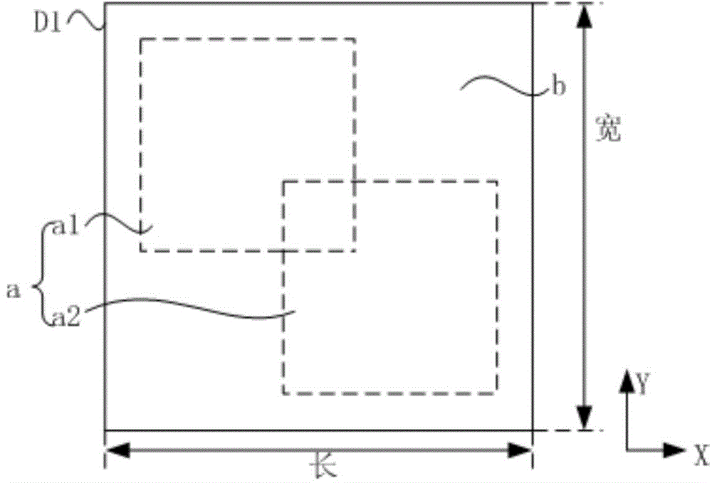
[0039] Figure 3A-Figure 3D It shows a schematic top view of the semiconductor device provided by Embodiment 1 of the present invention, please refer to Figure 3A-Figure 3D , the semiconductor device D1 includes: an active area a and an inactive area b, the active area a includes a plurality of active area units (such as: a1 and a2), and the plurality of active area units are in the The semiconductor device is staggered in the length direction, and the multiple active area units are staggered in the width direction of the semiconductor device.

[0040] In this embodiment, the length direction of the semiconductor device D1 is designated as the X direction, and the width direction of the semiconductor device D1 is designated as the Y direction, wherein the X direction is perpendicular to the Y direction.

[0041]The area other than the active area a is an inactive area. There are two-dimensional electron gas, electrons or holes under the active area a, which is the working ar...

Embodiment 2

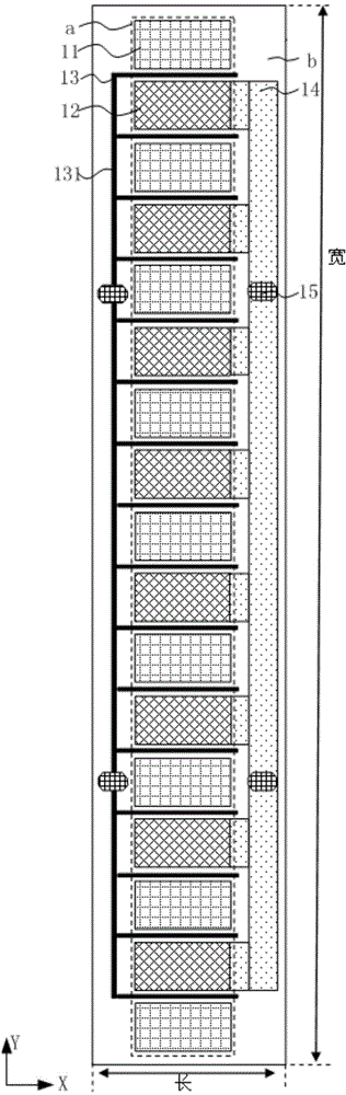
[0048] Figure 4 It shows a schematic top view of the semiconductor device provided by Embodiment 2 of the present invention, please refer to Figure 4 , the semiconductor device D2 includes: an active area and an inactive area b, the area outside the active area is an inactive area b, and the active area includes a plurality of active area units (such as: a1, a2 , a3 and a4), the plurality of active region units are staggered in the length direction of the semiconductor device, and the plurality of active region units are staggered in the width direction of the semiconductor device.

[0049] The active region of the semiconductor device D2 includes a plurality of active region units (such as: a1, a2, a3 and a4), and in the width direction of the semiconductor device, a plurality of active region units (such as: a1, a2, a3 and a4) Staggered arrangement, that is, each active region unit is repeatedly arranged in the width direction of the semiconductor device, and two adjacent...

Embodiment 3

[0060] Figure 6A-6E It shows a schematic top view of the semiconductor device provided by Embodiment 3 of the present invention. Embodiment 3 of the present invention is based on the above-mentioned embodiments, and the following combines Figure 6A-6E Embodiment 3 of the present invention will be described.

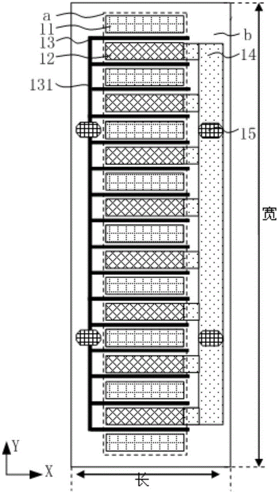
[0061] See Figure 6A ,exist Figure 6A Among them, the active area of ​​the semiconductor device D3 includes a plurality of active area units (such as: a1, a2, a3 and a4), and each active area unit includes a source 11, a gate 13 and a drain 12, The source 11, the gate 13 and the drain 12 form a local interdigitated structure in the active area unit, and any two adjacent active area units do not overlap in the length direction of the semiconductor device. The width direction of the semiconductor device overlaps (such as: a1 and a2). The advantage of this treatment is that the distance between two adjacent active region units in the width direction of the semiconduct...


PUM


Abstract

The invention discloses a semiconductor device and a manufacturing method thereof. The semiconductor device comprises an active region and a passive region, wherein the active region comprises a plurality of active region units; the multiple active region units are arranged in the length direction of the semiconductor device in a staggering manner, and are arranged in the width direction of the semiconductor device in the staggering manner. The overall length of the semiconductor device is increased, the radiating area of the semiconductor device is increased, the heat dissipation of heat is quickened, and the internal temperature in the semiconductor device is uniformly distributed; the width-length ratio of the entire semiconductor device is reduced, the influence of increase of the width-length ratio on the performance of the device is reduced, and the subsequent process difficulty can also be reduced.

Description

technical field [0001] The invention relates to the technical field of semiconductors, in particular to a semiconductor device and a manufacturing method thereof. Background technique [0002] Gallium nitride semiconductor devices have significant advantages such as large band gap, high electron mobility, high breakdown field strength, and high temperature resistance. They are suitable for the production of high temperature, high voltage, high frequency, and high power electronic devices, and have broad application prospects. [0003] See figure 1 , figure 1 Shows a schematic top view of a gallium nitride semiconductor device in the prior art, the gallium nitride semiconductor device shown includes an active region a and a passive region b, the active region a is in a closed form, and the region outside the active region a It is the passive region b, the source 11, the drain 12 and the gate 13 in the active region a are repeatedly arranged in the width direction of the dev...

Claims


Application Information

Patent Timeline
IPC IPC(8): H01L27/02H01L21/77
CPCH01L2924/0002H01L29/4175H01L29/41758H01L29/42316H01L29/1608H01L29/2003H01L29/778H01L2924/00H01L23/481H01L23/5286H01L29/0696H01L29/0847H01L29/16H01L29/1602H01L29/20H01L29/24
Inventor 张乃千刘飞航裴轶
Owner GPOWER SEMICON
Why Eureka
Try Eureka