
Superconducting thin film for single photon detection system and preparation method thereof

A technology of single-photon detection and superconducting thin film, which is applied in the field of single-photon detection, can solve the problems of easy peeling off of the film, uneven surface of the film, short circuit of the circuit, etc., and achieve automatic cutting, no photoresist residue, and convenient and accurate alignment Effect

Inactive Publication Date: 2015-05-13
SOUTHWEST JIAOTONG UNIV
View PDF5 Cites 7 Cited by
  • Summary
  • Abstract
  • Description
  • Claims
  • Application Information

AI Technical Summary

Problems solved by technology

The surface of the film prepared by the existing film preparation process is not smooth, the film is easy to fall off, and even the circuit is short-circuited due to the film not being etched clean during the etching process, which affects the normal use of the detector
In addition, in the process of cutting the above-mentioned superconducting thin film into small pieces, it is generally used to cut manually under a microscope, which is not easy to align; in some cases, the initial cutting position is determined first, and then semi-automatic cutting is realized by setting the cutting distance, which is difficult to achieve Automatic cutting

Method used


Image

  • Superconducting thin film for single photon detection system and preparation method thereof
  • Superconducting thin film for single photon detection system and preparation method thereof
  • Superconducting thin film for single photon detection system and preparation method thereof

Examples


Embodiment 1

[0027] Example 1: Preparation of niobium metal superconducting thin film

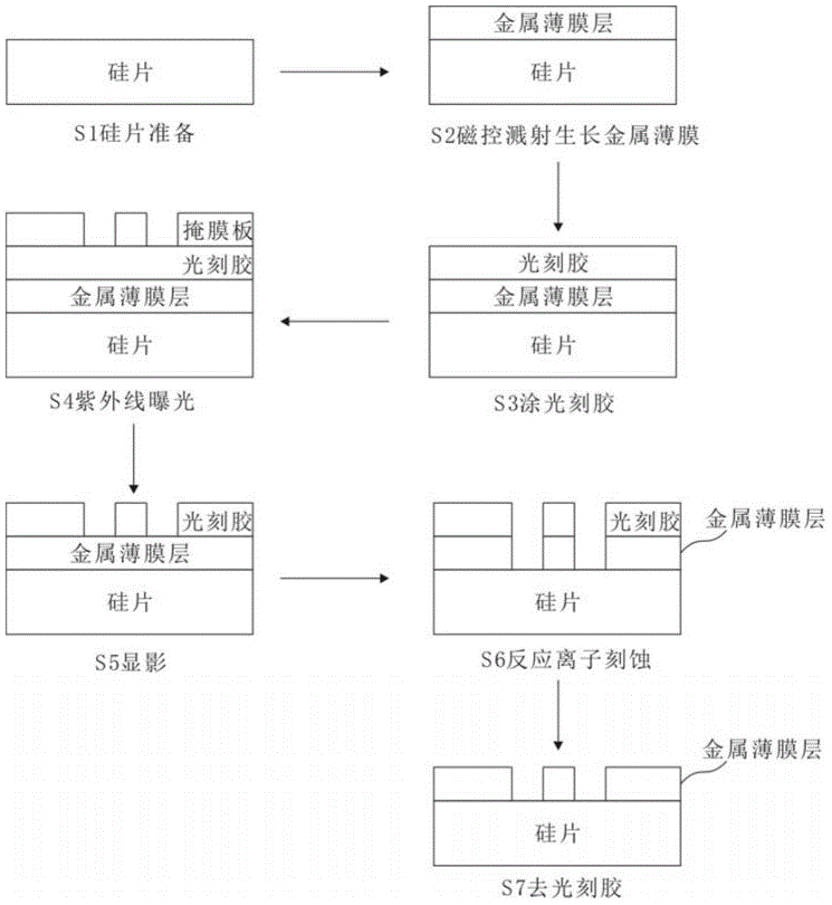
[0028] Such as figure 1 As shown, a method for preparing a niobium metal superconducting thin film for a single photon detection system comprises the following steps:

[0029] S1. Silicon wafer preparation: choose a round silicon wafer with a thickness of 500um and a diameter of 3 inches as the base material, clean the silicon wafer with an ultrasonic oscillator in acetone, ethanol, hydrofluoric acid and ultrapure water, and then air dry;

[0030] S2, grow one layer of niobium metal film on the silicon chip after cleaning, preferably, adopt magnetron sputtering process to grow niobium metal film, control film growth rate by controlling sputtering power size, sputtering power is 100 watts, then The film thickness is controlled by controlling the sputtering time, and the sputtering time is 5 minutes, and a layer of niobium metal film with a thickness of 160 nm is finally grown.

[0031] Compared with or...

Embodiment 2

[0041] Example 2: Preparation of Tungsten Metal Superconducting Thin Film

[0042] Such as figure 1 As shown, a method for preparing a tungsten metal superconducting thin film for a single photon detection system comprises the following steps:

[0043] S1. Silicon wafer preparation: choose a round silicon wafer with a thickness of 500um and a diameter of 3 inches as the base material, clean the silicon wafer with an ultrasonic oscillator in acetone, ethanol, hydrofluoric acid and ultrapure water, and then air dry;

[0044] S2, grow a layer of tungsten metal thin film on the silicon chip after cleaning, preferably, adopt magnetron sputtering technique to grow tungsten metal thin film, control film growth rate by controlling sputtering power size, sputtering power is 50 watts, then The film thickness is controlled by controlling the sputtering time, and the sputtering time is 10 minutes, and a tungsten metal thin film with a thickness of 160 nm is finally grown.

[0045]Compar...

Embodiment 3

[0055] Embodiment 3: Preparation of aluminum metal superconducting thin film.

[0056] Such as figure 1 Shown, a kind of preparation method of the aluminum metal superconducting thin film that is used for single-photon detection system comprises the following steps:

[0057] S1. Silicon wafer preparation: choose a round silicon wafer with a thickness of 500um and a diameter of 3 inches as the base material, clean the silicon wafer with an ultrasonic oscillator in acetone, ethanol, hydrofluoric acid and ultrapure water, and then air dry;

[0058] S2, grow a layer of aluminum metal thin film on the silicon chip after cleaning, preferably, adopt magnetron sputtering process to grow aluminum metal thin film, control film growth rate by controlling sputtering power size, sputtering power is 100 watts, then The film thickness is controlled by controlling the sputtering time, and the sputtering time is 1 minute, and a layer of aluminum metal film with a thickness of 160 nm is finall...


PUM

PropertyMeasurementUnit
diameteraaaaaaaaaa

Abstract

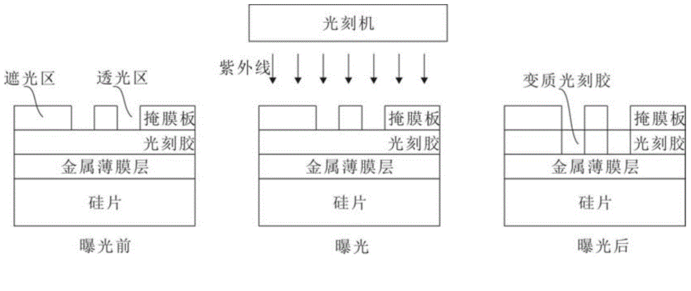
The invention discloses a preparation method for a single photon detection system; the preparation method comprises the following steps: S1, cleaning the silicon wafer; S2, growing the metal film on the silicon wafer by magnetron sputtering operation; S3, evenly coating a layer of photoresist on the surface of the metal film, baking and sizing; S4, using the prefab mask for covering the photoresist, using the ultraviolet ray for exposing the photoresist; S5, taking off the mask, using the developing liquid for etching the exposed part of the photoresist; S6, etching the exposed metal film part from the developed film; and S7, cleaning the etched film and air drying. A superconducting thin film for a single photon detection system is further disclosed, the film takes the silicon wafer as the substrate material, the material of the thin film is metal, and the locating mark is formed on the thin film for automatically cutting the sheet. The thin film prepared by the method has flat surface and is not easy to fall off, the photoresist has no residue, and the locating mark is formed on the thin film for exactly finding the position for the following cutting operation and the automatically cutting operation can be achieved.

Description

technical field [0001] The invention belongs to the technical field of single-photon detection, and in particular relates to a superconducting thin film used in a single-photon detection system and a preparation method thereof. Background technique [0002] A single photon detector is a device that is extremely sensitive to single quantum substances such as photons. It has a wide range of applications in physics, astronomical photometry, optical time domain reflectometry (OTDR), quantum key distribution system (QKD) and other fields. Since these detectors work in a temperature range below 1K, compared with ordinary semiconductor photon detectors (such as photomultiplier tubes and avalanche photodiodes), they are characterized by their unique high detection sensitivity and low background noise. , low dark count rate and fast signal response speed have become the best among photon detectors. [0003] In recent years, a transition-edge sensor (Transition-Edge Sensors, TES) ba...

Claims


Application Information

Patent Timeline
Patent Type & Authority Applications(China)
IPC IPC(8): H01L39/24H01L39/16H10N60/01H10N60/30
Inventor 常相辉刘想靓韦强郭伟杰李海杰周品嘉韦联福
Owner SOUTHWEST JIAOTONG UNIV
Learn More