Transparent organic light-emitting device and method for manufacturing same

A luminescence and electromechanical technology, applied in the direction of electrical solid devices, semiconductor/solid device manufacturing, electrical components, etc., can solve the problems of low light transmittance, easy cracks, thick transparent devices, etc., and achieve good compactness and uniformity , low deposition temperature and strong adhesion

Inactive Publication Date: 2015-05-20
OCEANS KING LIGHTING SCI&TECH CO LTD +2
View PDF0 Cites 1 Cited by
  • Summary
  • Abstract
  • Description
  • Claims
  • Application Information

AI Technical Summary

Problems solved by technology

As the desiccant in the transparent device absorbs a large amount of oxygen and water vapor, the desiccant loses its absorption capacity in a short period of time, resulting in the gradual accumulation of oxygen and water vapor in the transparent device, so that the life of the transparent device is significantly reduced, and the long life cannot be achieved. Encapsulation requirements for transparent organic electroluminescent devices
The light transmittance of the commonly used glass cover or metal cover is low, which will reduce the light extraction efficiency of transparent devices and affect the visual effect of transparent devices in practical applications
At the same time, the glass cover or metal cover usually used is a brittle material, which is prone to cracks, and the transparent device will appear very thick after packaging, which is not suitable for flexible transparent devices.

Method used


Image

  • Transparent organic light-emitting device and method for manufacturing same
  • Transparent organic light-emitting device and method for manufacturing same
  • Transparent organic light-emitting device and method for manufacturing same

Examples


Embodiment 1

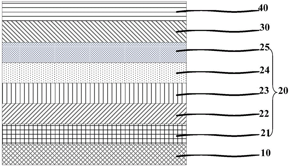
[0058] figure 1 It is a schematic structural view of the transparent organic electroluminescent device in Example 1; as figure 1As shown, the transparent organic electroluminescent device in Example 1 includes an ITO glass substrate (10), an organic light-emitting functional layer (20), a transparent cathode (30) and an encapsulation layer (40) stacked sequentially from bottom to top; The organic electroluminescent functional layer (20) includes a hole injection layer (21), a hole transport layer (22), a light emitting layer (23), an electron transport layer (24) and an electron injection layer ( 25). figure 2 yes figure 1 Schematic diagram of the structure of the encapsulation layer of the transparent organic electroluminescent device; as figure 2 As shown, the encapsulation layer (40) includes a mixed barrier layer (41), a first silicon oxynitride film layer (42), an inorganic barrier layer (43) and a second oxygen Silicon nitride film layer (44).

[0059] A method fo...

Embodiment 2

[0077] A method for preparing a transparent organic electroluminescent device, comprising the steps of:

[0078] (1), (2), (3) are the same as embodiment 1;

[0079] (4) Preparation of encapsulation layer:

[0080] a) Preparation of the mixed barrier layer: the mixed barrier layer was prepared on the surface of the transparent cathode by vacuum evaporation method, and the vacuum degree was 1×10 -5 Pa, the evaporation rate is The mixed barrier layer materials include N,N'-diphenyl-N,N'-di(1-naphthyl)-1,1'-biphenyl-4,4'-diamine (NPB) and doped in Aluminum fluoride (AlF 3 ) and neodymium fluoride (NdF 3 ); aluminum fluoride (AlF 3 ) The mass fraction is 20%, neodymium fluoride (NdF 3 ) is 10% by mass; the thickness of the mixed barrier layer is 200nm;

[0081] b) Preparation of the first silicon oxynitride film layer: the first silicon oxynitride film layer was prepared on the surface of the mixed barrier layer by plasma enhanced chemical vapor deposition, the working pre...

Embodiment 3

[0086] A method for preparing a transparent organic electroluminescent device, comprising the steps of:

[0087] (1), (2), (3) are the same as embodiment 1;

[0088] (4) Preparation of encapsulation layer:

[0089] a) Preparation of the mixed barrier layer: the mixed barrier layer was prepared on the surface of the transparent cathode by vacuum evaporation method, and the vacuum degree was 1×10 -5 Pa, the evaporation rate is Hybrid barrier materials include 8-hydroxyquinoline aluminum (Alq 3 ) and doped in 8-hydroxyquinoline aluminum (Alq 3 ) in magnesium fluoride (MgF 2 ) and gadolinium fluoride (GdF); magnesium fluoride (MgF 2 ) is 10% by mass, and gadolinium fluoride (GdF) is 20% by mass; the thickness of the mixed barrier layer is 100nm;

[0090] b) Preparation of the first silicon oxynitride film layer: the first silicon oxynitride film layer was prepared on the surface of the mixed barrier layer by plasma enhanced chemical vapor deposition, the working pressure wa...


PUM


Abstract

The invention discloses a transparent organic light-emitting device which comprises a packaging layer. The packaging layer comprises a mixed barrier layer, a first silicon oxynitride film layer, an inorganic barrier layer and a second silicon oxynitride film layer; the mixed barrier layer is made of organic compounds, first metal fluorides and second metal fluorides; the organic compounds include at least one type of TAPC, NPB, Alq<3>, m-MTDATA, BCP and TPBi; the first metal fluorides include at least one type of magnesium fluorides, aluminum fluorides and sodium aluminum fluorides; the second metal fluorides include at least one type of lanthanum fluorides, neodymium fluorides and gadolinium fluorides; the first silicon oxynitride film layer and the second silicon oxynitride film layer are made of silicon oxynitride; the inorganic barrier layer is made of at least one type of nitrogen-doped titanium oxides, nitrogen-doped magnesium oxides, nitrogen-doped silicon oxides, nitrogen-doped zirconium oxides, nitrogen-doped zinc oxides and nitrogen-doped aluminum oxides.

Description

technical field [0001] The invention relates to the technical field of organic electroluminescent devices, in particular to a transparent organic electroluminescent device and a preparation method thereof. Background technique [0002] For the existing organic electroluminescent devices (OLED), according to the different light emitting surfaces, it can be divided into three categories: bottom emitting organic electroluminescent devices (BOLED), top emitting organic electroluminescent devices (TEOLED) and transparent organic electroluminescent devices (TOLEDs). The difference between transparent organic electroluminescent device (TOLED) and top emitting organic electroluminescent device (TEOLED) and bottom organic electroluminescent device (BOLED) is that both the cathode and the anode are made of transparent materials, so that the light generated in the emitter The light is emitted from both the cathode and anode sides simultaneously. The transparent organic electrolumines...

Claims


Application Information

Patent Timeline
Patent Type & Authority Applications(China)
IPC IPC(8): H01L51/50H01L51/52H01L51/54H01L51/56
Inventor 周明杰钟铁涛王平陈吉星
Owner OCEANS KING LIGHTING SCI&TECH CO LTD
Why Eureka
Try Eureka