
Organic electroluminescence device and production method thereof
An electroluminescent device and electroluminescent technology, which can be used in organic light-emitting devices, organic light-emitting device structures, organic semiconductor devices, etc., and can solve the problems of poor mechanical strength, high cost, and heavy weight.
- Summary
- Abstract
- Description
- Claims
- Application Information
AI Technical Summary
Problems solved by technology
Method used
Image

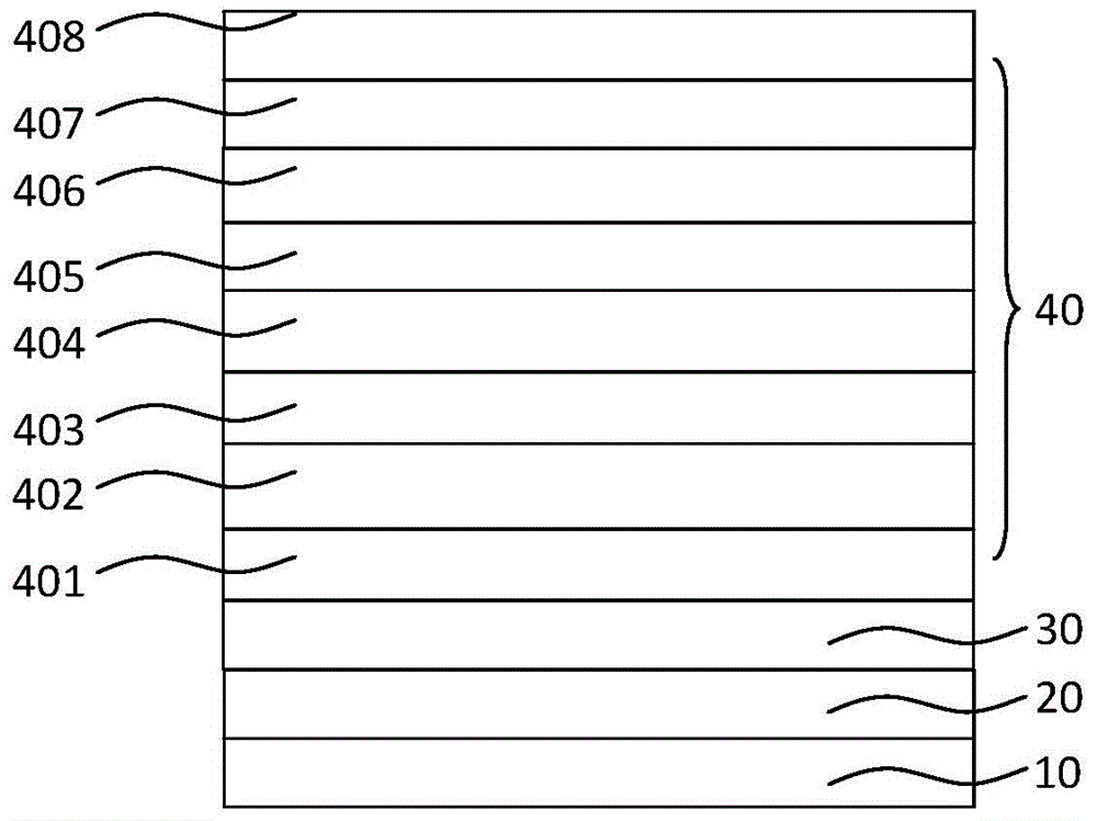
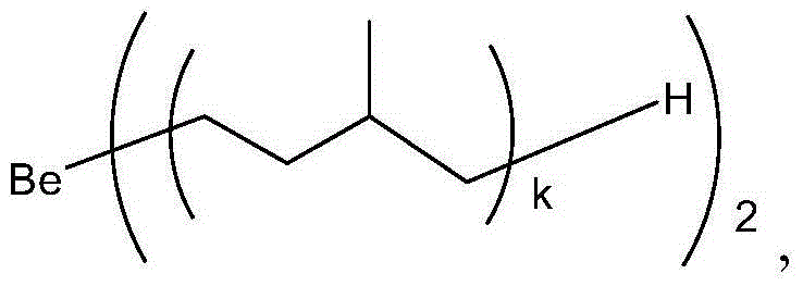
Examples
Embodiment 1
[0087] An organic electroluminescent device is prepared through the following steps:
[0088] (1) Provide a clean anode conductive substrate:
[0089] Clean the ITO glass substrate with acetone, ethanol, deionized water, and ethanol in an ultrasonic cleaner in sequence, wash and wash for 5 minutes in one item, then blow dry with nitrogen, and dry in an oven for later use; surface activation of the cleaned ITO glass processing; ITO thickness is 100nm;
[0090] (2) Vacuum evaporation of the luminescent functional layer on the ITO glass substrate:
[0091] Specifically, the light emitting functional layer includes a hole injection layer, a hole transport layer, a light emitting layer, an electron transport layer and an electron injection layer;
[0092] Preparation of the hole injection layer: the MoO 3 The mixture obtained by mixing with NPB according to the mass ratio of 3:7 is used as the material of the hole injection layer, the thickness is 10nm, and the vacuum degree is ...
Embodiment 2
[0110] An organic electroluminescent device is prepared through the following steps:
[0111] (1), (2), (3) are the same as embodiment 1;
[0112] (4) Prepare the encapsulation layer on the outside of the cathode:
[0113] The encapsulation layer is an alternately stacked inorganic barrier layer and a mixed barrier layer;
[0114] Fabrication of the inorganic barrier layer: the organic electroluminescent device sample prepared with the cathode is placed in the deposition chamber of the atomic layer deposition system, and then,
[0115] (a) The metal source Mg(CpEt) 2 Inject nitrogen into the deposition chamber and deposit on the cathode, the injection time is 20ms, and the nitrogen flow rate is 20sccm;
[0116] (b) Inject nitrogen gas to flush the deposition chamber, the injection time is 10s, and the flow rate is 20 sccm;
[0117] (c) Water vapor is then injected into the deposition chamber along with nitrogen gas to react with the metal source. The injection time is 20 m...
Embodiment 3
[0123] An organic electroluminescent device is prepared through the following steps:
[0124] (1), (2), (3) are the same as embodiment 1;
[0125] (4) Prepare the encapsulation layer on the outside of the cathode:
[0126] The encapsulation layer is an alternately stacked inorganic barrier layer and a mixed barrier layer;
[0127] Fabrication of the inorganic barrier layer: the organic electroluminescent device sample prepared with the cathode is placed in the deposition chamber of the atomic layer deposition system, and then,
[0128] (a) The metal source Ca(CpEt) 2 Inject nitrogen into the deposition chamber and deposit on the cathode, the injection time is 10ms, and the nitrogen flow rate is 10sccm;
[0129] (b) Inject nitrogen gas to flush the deposition chamber, the injection time is 5s, and the flow rate is 10 sccm;
[0130] (c) Water vapor is then injected into the deposition chamber along with nitrogen gas to react with the metal source. The injection time is 10 ms...
PUM
 Abstract
Description
Claims
Application Information