Organic electroluminescence device and preparation method thereof
An electroluminescent device and electroluminescent technology, which are applied in the fields of electro-solid devices, semiconductor/solid-state device manufacturing, electrical components, etc., can solve the problems of refractive index difference, total reflection loss, low light output performance, etc. The effect of enhancing the scattering of light and increasing the transmission rate
- Summary
- Abstract
- Description
- Claims
- Application Information
AI Technical Summary
Problems solved by technology
Method used
Image

Examples
preparation example Construction
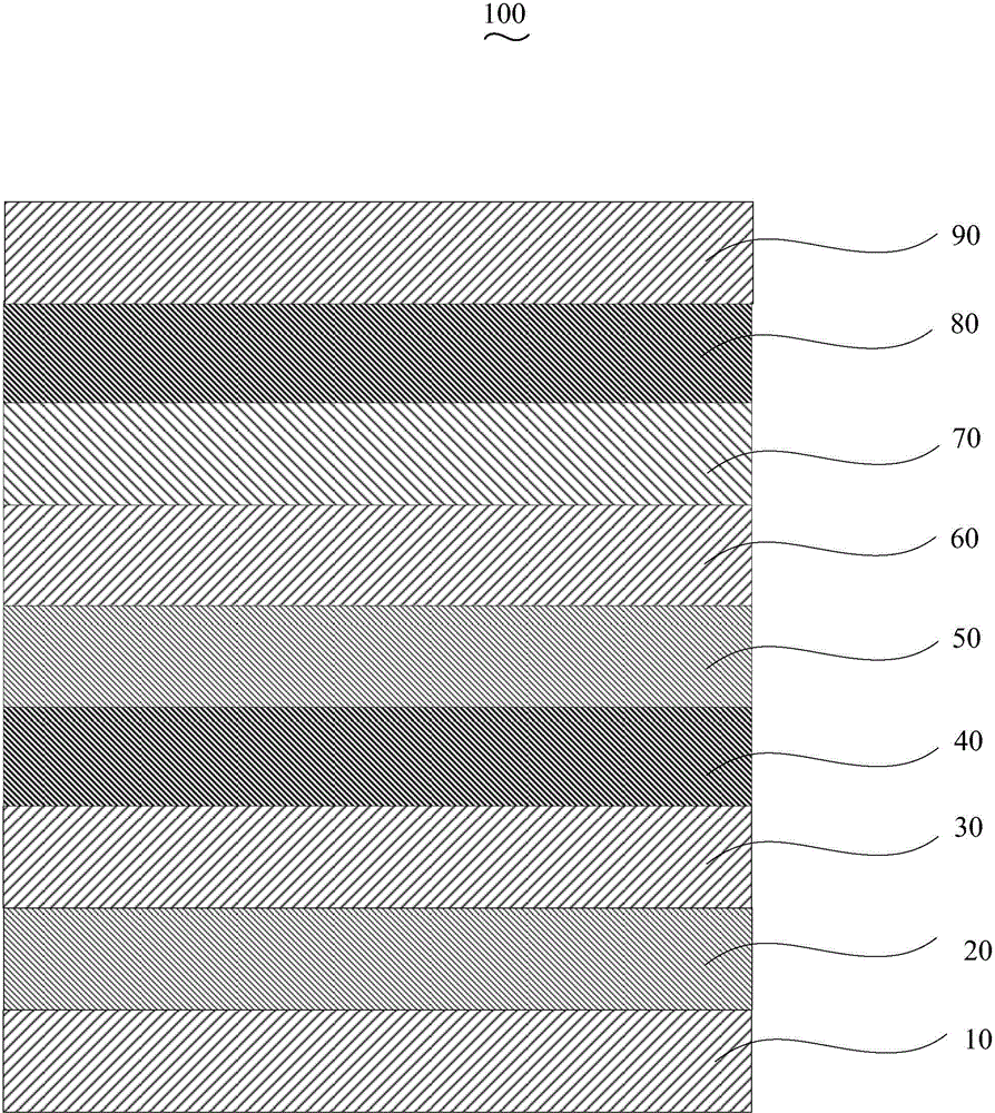
[0038] The manufacturing method of the organic electroluminescent device 100 of an embodiment includes the following steps:
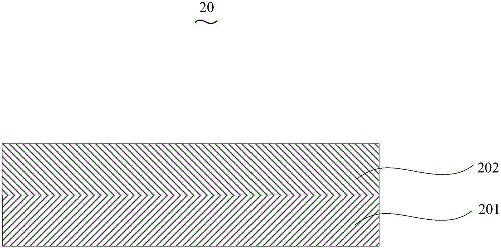
[0039] In step S110, the scattering layer 20 is prepared by electron beam evaporation on the surface of the glass substrate 10.
[0040] The scattering layer 20 is formed on one side surface of the glass substrate 10. The scattering layer 20 is composed of a ternary doped layer 201 and a hole transport material doped layer 202. The ternary doped layer 201 is prepared on the surface of the glass substrate 10 by electron beam evaporation. The ternary doped layer 201 includes Luminescent material, organic silicon small molecule material and copper compound material, the luminescent material is selected from 4-(dinitrile methyl)-2-butyl-6-(1,1,7,7-tetramethylgyura Methidine-9-vinyl)-4H-pyran (DCJTB), 9,10-di-β-naphthyleneanthracene (ADN), 4,4'-bis(9-ethyl-3-carbazole vinyl) Base) -1,1'-biphenyl (BCzVBi) and 8-hydroxyquinoline aluminum (Alq 3 ), the energy gap ...
Embodiment 1
[0061] The structure prepared in this embodiment is a glass substrate / Alq 3 :UGH2:CuI / TAPC:MgF 2 / ITO / MoO 3 / NPB / Alq 3 / TAZ / CsF / Ag organic electroluminescence device. In this embodiment and the following embodiments, " / " means layer, and ":" means doping.
[0062] The glass substrate is N-LASF44. After the glass substrate is rinsed with distilled water and ethanol, it is soaked in isopropanol overnight. A scattering layer is prepared on a glass substrate. The scattering layer is composed of a ternary doped layer and a hole transport material doped layer. The ternary doped layer is prepared by electron beam evaporation on the surface of the glass substrate. The material is Alq 3 :UGH2:CuI, Alq 3 The mass ratio of UGH2 to CuI is 10:3:1 and the thickness is 400nm. The cesium salt material doped layer is prepared by thermal resistance evaporation on the ternary doped surface, the material is TAPC:MgF 2 , TAPC and MgF 2 The mass ratio is 9:1 and the thickness is 160nm. Then, ITO is pre...
Embodiment 2
[0070] The preparation structure of this embodiment is a glass substrate / ADN: UGH1: Cu 2 O / TCTA:MgO / IZO / V 2 O 5 / TAPC / DCJTB / TAZ / Cs 2 CO 3 / Al organic electroluminescent device.
[0071] The glass substrate is N-LAF36. After the glass substrate is rinsed with distilled water and ethanol, it is soaked in isopropanol for one night to prepare a scattering layer on the glass substrate. The scattering layer is doped with a ternary doped layer and hole transport material Layer composition, using electron beam evaporation to prepare ternary doping on the surface of the glass substrate, the material is ADN:UGH1:Cu 2 O, AND, UGH1 and Cu 2 The mass ratio of O is 4:1:1 and the thickness is 600nm. The cesium salt material doped layer is prepared by thermal resistance evaporation on the ternary doped surface. The material is TCTA:MgO, and the mass ratio of TCTA to MgO is 7:1 , The thickness is 100nm. Then IZO is prepared on the scattering layer, the thickness is 80nm, and it is prepared by mag...
PUM
 Abstract
Description
Claims
Application Information
 - R&D
- Intellectual Property
- Life Sciences
- Materials
- Tech Scout
- Unparalleled Data Quality
- Higher Quality Content
- 60% Fewer Hallucinations
Browse by: Latest US Patents, China's latest patents, Technical Efficacy Thesaurus, Application Domain, Technology Topic, Popular Technical Reports.
© 2025 PatSnap. All rights reserved.Legal|Privacy policy|Modern Slavery Act Transparency Statement|Sitemap|About US| Contact US: help@patsnap.com