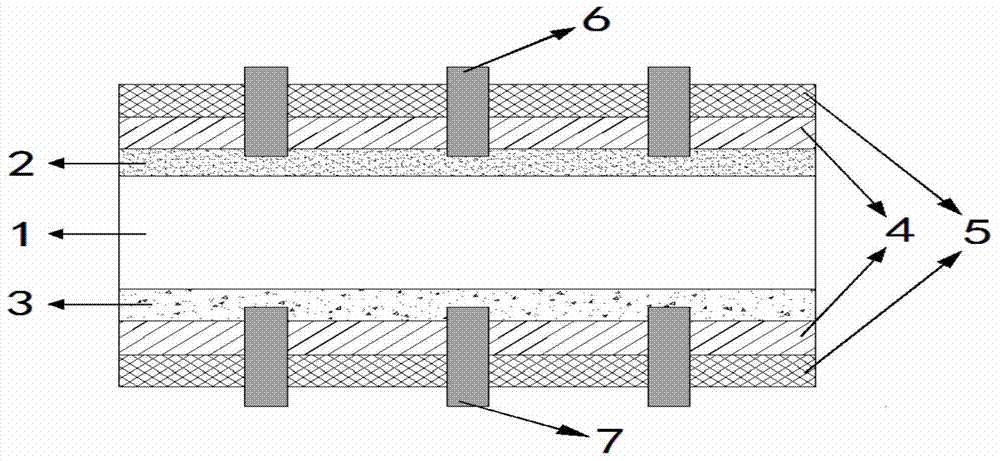
High efficiency N-type double-faced solar cell and preparation method thereof
A double-sided solar cell, N-type technology, which is applied in the field of solar cells to achieve the effects of high efficiency, easy operation, and increased open circuit voltage
- Summary
- Abstract
- Description
- Claims
- Application Information
AI Technical Summary
Problems solved by technology
Method used
Image
Examples
Embodiment 1
[0044] The preparation method of the above-mentioned N-type double-sided solar cell comprises the following steps:
[0045] (1) Select an N-type single crystal raw silicon wafer with a resistivity of 1-12Ω·cm, dilute it with a mixture of hydrogen peroxide and ammonia water, and then treat it at 60-80°C for 3-10min to remove the mechanical properties on the surface of the silicon wafer. damage layer. After the above-mentioned treatment, the silicon wafer is corroded with potassium hydroxide solution and texturing buffer with a concentration of 1.6-2.0% and a temperature of 70-90 ° C. The time is controlled at 20-30 minutes, and then washed with diluent hydrofluoric acid. Finally, a pyramid-shaped suede structure is obtained.
[0046] (2) On the front side of the double-sided textured silicon wafer, an n+ diffusion layer is formed by doping, and the diffusion method is boron tribromide (BBr 3 ) source tube diffusion, or ion implantation method, or spray boron source on-line di...
Embodiment 2
[0056] The preparation method of the above-mentioned N-type double-sided solar cell comprises the following steps:
[0057] (1) Select an N-type single crystal raw silicon wafer with a resistivity of 1-12Ω·cm, dilute it with a mixture of hydrogen peroxide and ammonia water, and then treat it at 60-80°C for 3-10min to remove the mechanical properties on the surface of the silicon wafer. damage layer. After the above-mentioned treatment, the silicon wafer is corroded with potassium hydroxide solution and texturing buffer with a concentration of 1.6-2.0% and a temperature of 70-90 ° C. The time is controlled at 20-30 minutes, and then washed with diluent hydrofluoric acid. Finally, a pyramid-shaped suede structure is obtained.
[0058] (2) On the front side of the double-sided textured silicon wafer, an n+ diffusion layer is formed by doping, and the diffusion method is boron tribromide (BBr 3 ) source tube diffusion, or ion implantation method, or spray boron source on-line di...
PUM
| Property | Measurement | Unit |
|---|---|---|
| Resistivity | aaaaa | aaaaa |
| Film thickness | aaaaa | aaaaa |
| Film thickness | aaaaa | aaaaa |
Abstract
Description
Claims
Application Information
