High-dielectric-constant gate dielectric composite channel field effect transistor and preparing method thereof

A technology with high dielectric constant and gate dielectric, applied in transistors, semiconductor/solid-state device manufacturing, circuits, etc., can solve the problems of high device power consumption, low ZnO channel mobility, and high operating voltage

Inactive Publication Date: 2015-07-08
TSINGHUA UNIV
View PDF2 Cites 25 Cited by
  • Summary
  • Abstract
  • Description
  • Claims
  • Application Information

AI Technical Summary

Problems solved by technology

However, the device structure uses SiO 2 As a back gate dielectric, therefore, the operating voltage is high (greater than 20V), resulting in a large power consumption of the device; at the same time, due to the relatively low mobility of the ZnO channel, the mobility of the composite channel is also low.

Method used


Image

  • High-dielectric-constant gate dielectric composite channel field effect transistor and preparing method thereof
  • High-dielectric-constant gate dielectric composite channel field effect transistor and preparing method thereof
  • High-dielectric-constant gate dielectric composite channel field effect transistor and preparing method thereof

Examples


preparation example Construction

[0043] Graphene / MoS of the above-mentioned high dielectric constant gate dielectric proposed by the present invention 2 The preparation method of the composite channel field effect transistor device, as shown in Figure 2, mainly includes the following steps:

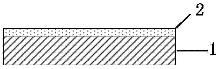
[0044] 1. Clean Si substrate 1: Boil Si substrate 1 with a mixture of hydrogen peroxide and concentrated sulfuric acid at a ratio of 1:4 at 80-85°C for 10-15 minutes to remove surface stains, and then rinse with deionized water for 10-10 minutes. 15min, dry for later use.

[0045] 2. Atomic layer deposition (ALD) is adopted on a Si substrate 1 with a thickness of 300 μm±0.05 μm, the temperature of the heat source (Hf source or Al source) is 80°C, the temperature of the cavity is 200°C, and the growth rate is 0.1nm per Prepared in a cyclic environment, the back gate high-k dielectric uses HfO 2 or Al 2 o 3 , thickness 10 ~ 25nm.

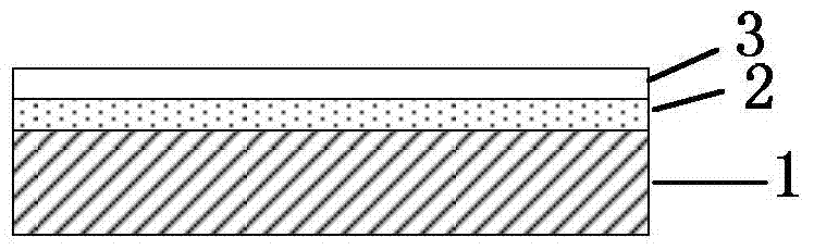
[0046] 3. Transfer the single-layer graphene 3 grown by CVD to the grown HfO with a thi...

Embodiment 1

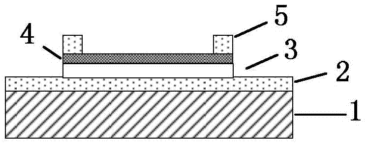
[0052] Graphene / MoS of high dielectric constant gate dielectric in this embodiment 2 Composite channel field effect transistor devices include sequentially stacked substrates, high dielectric constant (high k) gate dielectrics, patterned graphene conductive channels, patterned MoS 2 A thin film conduction channel, and a metal source electrode and a metal drain electrode on the compound conduction channel. Among them, the substrate is an N-type phosphorus-doped single-throw silicon substrate with a (100) crystal orientation, a resistivity of 0.006-0.009Ω·cm, and a thickness of 300μm±0.05μm; a high dielectric constant (high k) gate dielectric Using HfO 2 ; The thickness of single-layer graphene is 0.4nm ~ 0.6nm; MoS 2 Film thickness is 1.5~2nm

[0053] The source-drain electrodes 5 and 6 adopt a chromium (Cr) / gold (Au) stack structure with a thickness of 10-20nm / 50-60nm;

[0054] Its preparation method of the present embodiment, concrete technological process is as follows: ...

Embodiment 2

[0062] In this embodiment, graphene / MoS based on high dielectric constant gate dielectric is produced 2 Composite channel field effect transistor device and its preparation method are similar to embodiment one, the difference is that the back gate dielectric HfO with a thickness of 20nm is grown on the substrate Si1 2 2;


PUM

PropertyMeasurementUnit
thicknessaaaaaaaaaa
thicknessaaaaaaaaaa
thicknessaaaaaaaaaa

Abstract

The invention relates to a high-dielectric-constant gate dielectric composite channel field effect transistor device and belongs to the technical field of micro-electronics new materials and devices. The device comprises a substrate, a high-dielectric-constant gate dielectric, a graphical graphene conducting channel and a graphical molybdenum sulfide (MoS2) conducting channel which are sequentially stacked, and comprises a metal source electrode and a metal drain electrode which are arranged on the composite conducting channel. According to a preparing method, the mode of the atomic layer deposition technology (ALD) is directly utilized, and a high-dielectric-constant (high-k) material grows on the Si substrate. As the graphene/ molybdenum sulfide (MoS2) composite channels are adopted, the larger migration rate and the larger switch ratio can be obtained, and the electric property of the device is improved.

Description

technical field [0001] The invention belongs to the technical field of microelectronic devices, in particular to the preparation of a graphene / molybdenum sulfide composite channel field effect transistor device based on a high dielectric constant gate dielectric. Background technique [0002] Field-effect transistors are referred to as field-effect transistors for short, because they only rely on the majority of carriers in the semiconductor to conduct electricity, also known as unipolar transistors, which are voltage-controlled semiconductor devices. Its working principle is that when the gate voltage is applied, an electric field is generated in the gate insulating layer, and induced charges are generated on the surface of the semiconductor, and the carrier migration in the channel is regulated by the vertical electric field. Field effect transistors have high input resistance, low noise, low power consumption, large dynamic range, easy integration, no secondary breakdown ...

Claims


Application Information

Patent Timeline
Patent Type & Authority Applications(China)
IPC IPC(8): H01L29/78H01L29/786H01L21/04
CPCH01L29/78H01L21/20H01L29/1033H01L29/66477
Inventor 谢丹张丞徐建龙孙翊淋张小稳赵远帆李晓李昕明朱宏伟
Owner TSINGHUA UNIV
Why Eureka
Try Eureka