Anti-reflective micro-nano structure of sapphire surface and preparation method thereof

A micro-nano structure and sapphire technology, applied in the field of optical windows, can solve the problems of poor film adhesion, permeation and diffusion, and high overall cost, and achieve obvious anti-reflection and anti-reflection and hydrophilic self-cleaning. graphic distortion effect

Active Publication Date: 2015-08-19
HARBIN INST OF TECH SHENZHEN GRADUATE SCHOOL
View PDF6 Cites 22 Cited by
  • Summary
  • Abstract
  • Description
  • Claims
  • Application Information

AI Technical Summary

Problems solved by technology

The preparation of anti-reflection sub-wavelength micro-nano structures on the surface of sapphire can reduce the reflection of light, improve the light transmittance, and has the characteristics of wide field of view and wide-band high transmission, which can overcome many shortcomings of traditional anti-reflection coatings: such as coating Problems such as poor adhesion, easy erosion and permeation and diffusion
But in general, dry etching is easy to cause certain pollution and damage to the sapphire surface, especially the edge of the table.
More importantly, due to the high hardness of sapphire, the ICP etching machine used to etch sapphire in the test is more expensive than the general etching machine; it also needs to prepare an etching mask, and the overall cost of the test is high

Method used


Image

  • Anti-reflective micro-nano structure of sapphire surface and preparation method thereof
  • Anti-reflective micro-nano structure of sapphire surface and preparation method thereof
  • Anti-reflective micro-nano structure of sapphire surface and preparation method thereof

Examples


Embodiment 1

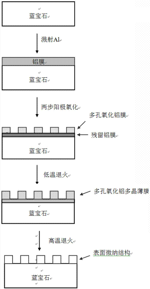
[0036] Step A: Prepare a layer of metal aluminum film on the surface of sapphire: sputter a layer of aluminum film with a thickness of about 1 μm on the surface of sapphire by magnetron sputtering;

[0037] Step B: Anodizing the aluminum film on the surface of the sapphire into an aluminum oxide film with a uniform and orderly porous surface, the anodizing is carried out in 0.3mol / L oxalic acid electrolytic solution, the oxidation temperature is 0°C, and the oxidation voltage is 40V; It is generally divided into the first anodic oxidation, chemical melting film, the second anodic oxidation and hole expansion process. The first anodic oxidation time is 30min; the chemical melting film is carried out in a mixture of 6wt.% phosphoric acid and 1.8wt.% chromic acid at 60°C for 10min; the second oxidation time is also 30min; The pores were expanded in phosphoric acid solution, and the expansion time was 40 minutes.

[0038] Step C: Low-temperature heat treatment: put the sapphire s...

Embodiment 2

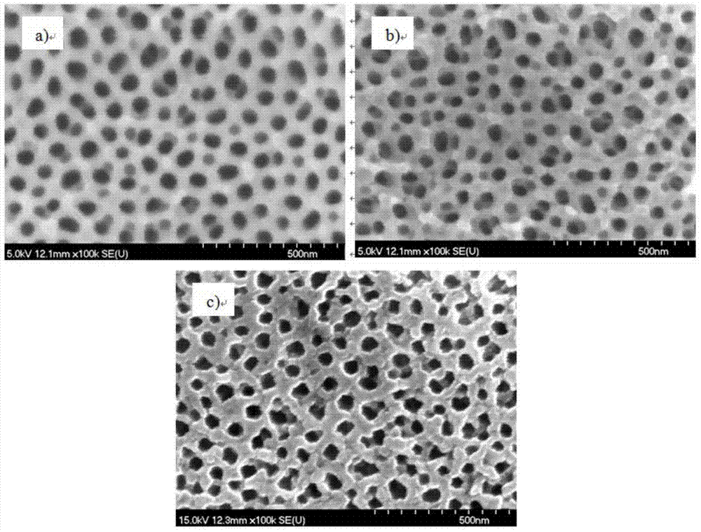
[0040] The difference between Example 2 and Example 1 is that step B is changed to directly expand the holes after one anodic oxidation, and other steps remain unchanged.

Embodiment 3

[0041] The difference between Example 3 and Example 1 is that only the anodizing temperature of step B is changed to 15° C., and other steps remain unchanged.


PUM

PropertyMeasurementUnit
thicknessaaaaaaaaaa
pore sizeaaaaaaaaaa
depthaaaaaaaaaa

Abstract

The invention provides an anti-reflective micro-nano structure of sapphire surface and a preparation method thereof. The method comprises the following steps: preparing a layer of metal aluminium membrane on surface of the sapphire; performing twice anodization on the metal aluminium membrane to form an ordered porous alumina film with uniform surface; and performing a two-step heat treatment on the porous alumina film to form the sapphire with surface having the poriform micro-nano structure. The preparation method has the advantages of simple process and can obviously reduce the preparation cost; the prepared sapphire has the micro-nano structure on the surface, has obvious anti-reflective anti-reflection effect on visible light or middle-infrared band, and self cleaning property for the surface is better.

Description

technical field [0001] The invention relates to the field of optical windows, in particular to a sapphire surface anti-reflection micro-nano structure and a preparation method thereof. Background technique [0002] Sapphire, also known as alumina single crystal, has excellent comprehensive mechanical, physical and chemical properties, such as high hardness, stable chemical properties, and good wave transmittance in the wide range of ultraviolet-visible light-medium wave infrared, so it can be used It is used to prepare various optical components, such as: optical detection window, display screen and touch screen panel, etc. However, compared with the current optical glass, sapphire has a large surface light reflection loss (double-sided reflectance R=14.3%) due to the large refractive index (1.77550nm) of the material itself, and the transmittance is less than 86.0%. , limiting the wider application of sapphire. What's more serious is that the service environment of the in...

Claims


Application Information

Patent Timeline
Patent Type & Authority Applications(China)
IPC IPC(8): C23C14/18C25D11/04C25D11/18B82Y40/00
Inventor 汪桂根韩杰才王立彦
Owner HARBIN INST OF TECH SHENZHEN GRADUATE SCHOOL
Why Eureka
Try Eureka