A method for preparing nano-dielectric layer based on oxygen plasma process
A technology of oxygen plasma and dielectric layer, which is used in semiconductor/solid-state device manufacturing, semiconductor devices, electrical components, etc., can solve the problems of affecting rectification function, interface defects, and high cost of device manufacturing process
- Summary
- Abstract
- Description
- Claims
- Application Information
AI Technical Summary
Problems solved by technology
Method used
Image

Examples
Embodiment Construction
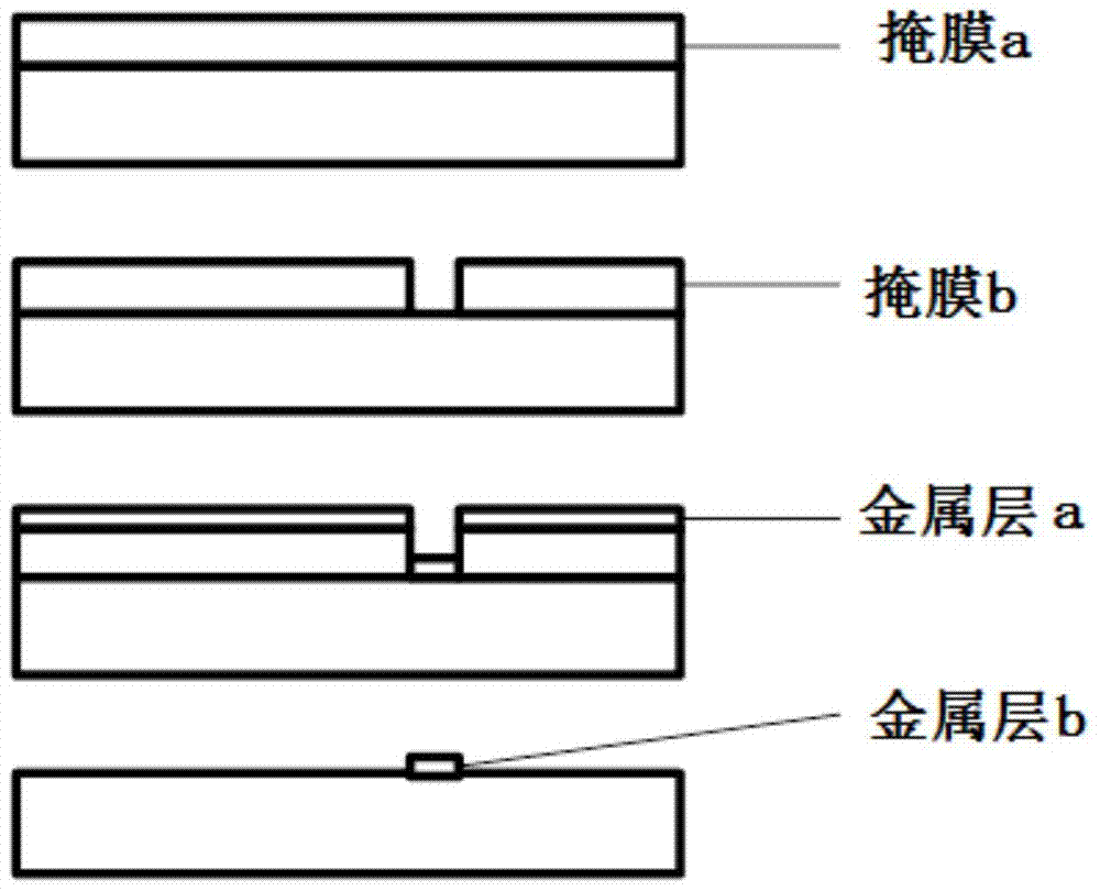
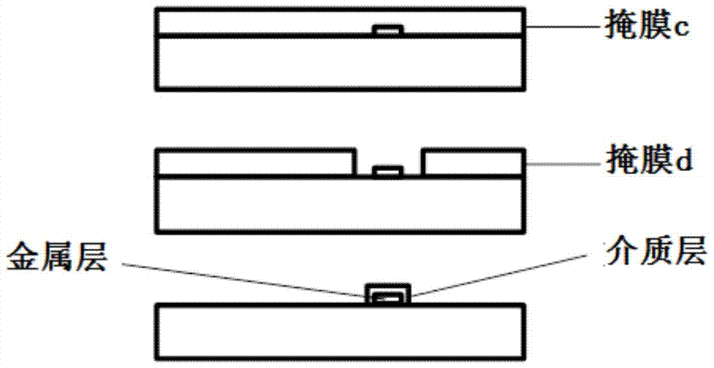
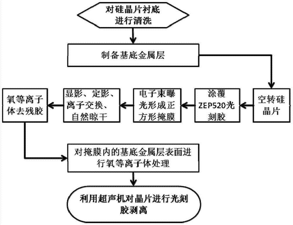
[0030] The present invention will be further described below in conjunction with accompanying drawing and two examples.
[0031] 1) Substrate cleaning
[0032] 11) The wafer used for the substrate is a silicon wafer with a 2 μm silicon dioxide layer. The specific cleaning steps are as follows: using an ultrasonic machine, soak the silicon wafer in acetone and sonicate at 40% power for 15 minutes, soak the silicon wafer in isopropanol and sonicate at 40% power for 15 minutes, wash it with deionized water, and dry it;
[0033] 12) Soak the silicon wafer in a mixture of concentrated sulfuric acid and hydrogen peroxide (5:1), heat it at 70°C for 15 minutes, and wash it with deionized water;
[0034] 13) Soak the silicon wafer in a mixture of water, hydrogen peroxide and ammonia (7:2:1), and heat at 70°C for 15 minutes;
[0035] 14) Soak the silicon wafer in a mixture of water, hydrogen peroxide and concentrated hydrochloric acid (7:2:1), heat at 70°C for 15min, wash with deioniz...
PUM
| Property | Measurement | Unit |
|---|---|---|
| thickness | aaaaa | aaaaa |
| thickness | aaaaa | aaaaa |
Abstract
Description
Claims
Application Information
 - R&D
- Intellectual Property
- Life Sciences
- Materials
- Tech Scout
- Unparalleled Data Quality
- Higher Quality Content
- 60% Fewer Hallucinations
Browse by: Latest US Patents, China's latest patents, Technical Efficacy Thesaurus, Application Domain, Technology Topic, Popular Technical Reports.
© 2025 PatSnap. All rights reserved.Legal|Privacy policy|Modern Slavery Act Transparency Statement|Sitemap|About US| Contact US: help@patsnap.com