Unlock instant, AI-driven research and patent intelligence for your innovation.

Encapsulation structure and encapsulation method of optoelectronic device

A technology of optoelectronic devices and packaging methods, which is applied in the field of optoelectronics, can solve the problems of device performance degradation, stability degradation, black spots, etc., and achieve the effects of excellent device performance, extended device life, and good curing agent properties

Inactive Publication Date: 2015-09-09
UNIV OF ELECTRONIC SCI & TECH OF CHINA
View PDF3 Cites 0 Cited by
  • Summary
  • Abstract
  • Description
  • Claims
  • Application Information

AI Technical Summary

Problems solved by technology

Oxygen oxidizes organic materials to generate carbonyl compounds, which are serious quenchers. In addition, black spots will be formed when materials deteriorate, accompanied by device performance degradation
The influence of water vapor is more obvious, and its main damage method is the hydrolysis of the organic layer compound by the conductive electrode, which greatly reduces the stability

Method used


Image

  • Encapsulation structure and encapsulation method of optoelectronic device
  • Encapsulation structure and encapsulation method of optoelectronic device
  • Encapsulation structure and encapsulation method of optoelectronic device

Examples


Embodiment 1

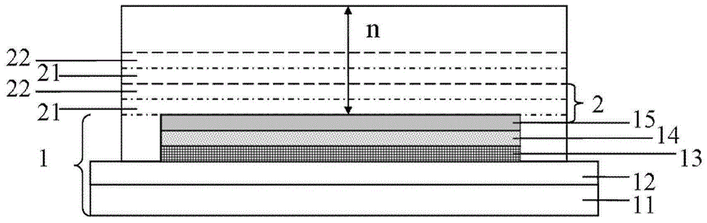
[0035] Such as figure 1 As shown, 1 is an organic electroluminescent device, the anode layer 12 is ITO, and the hole transport layer 13 is N,N'-bis(naphthylidene-1-yl)-N,N'-bis(phenyl) - benzidine (NPB), electron transport layer 14 is 1,3,5-(triN-phenyl-2-benzimidazole-2) benzene 41 (TPBi), cathode layer 15 is Mg:Ag alloy, inorganic package Material layer 21 is Al 2 o 3 , the UV-curable resin layer 22 includes 70% shellac, 15% reaction diluent and 15% triarylsulfur-type hexafluoroantimony salt, the number of cycles n is 20, and the device structure is:

[0036] Glass substrate / ITO / NPB(50nm) / TPBi(30nm) / Mg:Ag(200nm) / [Al 2 o 3 (200nm) / UV curable resin (100nm)] 20

[0037] The preparation method is as follows:

[0038] ①Use detergent, acetone solution, ethanol solution and deionized water to ultrasonically clean the substrate and dry it with nitrogen;

[0039] ②Transfer the clean substrate to the high vacuum evaporation chamber, and keep the pressure of the organic cavity ...

Embodiment 2

[0046] Such as figure 1 As shown, 1 is an organic electroluminescent device, the anode layer 12 is ITO, and the hole transport layer 13 is N,N'-bis(naphthylidene-1-yl)-N,N'-bis(phenyl) - benzidine (NPB), electron transport layer 14 is 1,3,5-(triN-phenyl-2-benzimidazole-2) benzene 41 (TPBi), cathode layer 15 is Mg:Ag alloy, inorganic package Material layer 21 is Al 2 o 3 , the UV-curable resin layer 22 includes 82% shellac, 10% reaction diluent and 8% triarylsulfur-type hexafluoroantimony salt, the number of cycles n is 16, and the device structure is:

[0047] Glass substrate / ITO / NPB(50nm) / TPBi(30nm) / Mg:Ag(200nm) / [Al 2 o 3 (200nm) / UV curable resin (100nm)] 16

[0048] The preparation method is similar to Example 1.

Embodiment 3

[0050] Such as figure 1 As shown, 1 is an organic electroluminescent device, the anode layer 12 is ITO, and the hole transport layer 13 is N,N'-bis(naphthylidene-1-yl)-N,N'-bis(phenyl) - benzidine (NPB), electron transport layer 14 is 1,3,5-(triN-phenyl-2-benzimidazole-2) benzene 41 (TPBi), cathode layer 15 is Mg:Ag alloy, inorganic package Material layer 21 is Al 2 o 3 , the UV-curable resin layer 22 includes 85% shellac, 10% reaction diluent and 5% triarylsulfur hexafluoroantimony salt, the number of cycles n is 12, and the device structure is:

[0051] Glass substrate / ITO / NPB(50nm) / TPBi(30nm) / Mg:Ag(200nm) / [Al 2 o 3 (200nm) / UV curable resin (100nm)] 12

[0052] The preparation method is similar to Example 1.


PUM


Abstract

The invention discloses an encapsulation structure and encapsulation method of an optoelectronic device. The encapsulation structure includes a film encapsulation layer coating the optoelectronic device; inorganic encapsulation material layers and ultraviolet light cured resin layers are alternately superimposed periodically for n periods so as to form the film encapsulation layer, wherein n satisfies the expression that 1<=n<=20. The ultraviolet light cured resin is composed of the following components by mass percentage: shellac; reactive diluent; and triaryl sulfur type hexafluoro antimonic salt. With the encapsulation structure adopted, oxygen and water in the surrounding environment can be effectively blocked, and the improvement of the stability of the device can be benefitted, and the service life of the device can be prolonged. The encapsulation method has the advantages of simple preparation process and low cost.

Description

technical field [0001] The invention relates to the field of optoelectronic technology, in particular to a packaging structure and a packaging method of an optoelectronic device. Background technique [0002] With the rapid development of global high-tech, after microelectronics technology, optoelectronics technology has gradually become a hot spot in global industrialization and research. With the rapid development of optoelectronic technology, optoelectronic products such as light-emitting diodes, organic light-emitting diodes, solar cells, and thin-film transistors have become more mature and have entered people's lives, greatly improving people's quality of life. At the same time, the wide application of optoelectronic information technology in various fields of social life has also created a huge growing market, and the competition in the field of optoelectronic information is unfolding worldwide. [0003] Current optoelectronic devices, including organic electrolumine...

Claims


Application Information

Patent Timeline
IPC IPC(8): H01L51/52H01L51/44H01L51/10
CPCH10K10/88H10K30/88H10K50/8445H10K2102/00Y02E10/549
Inventor 于军胜王煦郑丁韩世蛟
Owner UNIV OF ELECTRONIC SCI & TECH OF CHINA
Features
  • R&D
  • Intellectual Property
  • Life Sciences
  • Materials
  • Tech Scout
  • Unparalleled Data Quality
  • Higher Quality Content
  • 60% Fewer Hallucinations
Learn More