Method for rapidly growing large-size high-purity semi-insulating silicon carbide single crystal

A silicon carbide single crystal, semi-insulating technology, applied in chemical instruments and methods, single crystal growth, crystal growth and other directions, can solve the problems of reducing Al, difficult to reduce, low production efficiency, etc., to improve productivity and reduce nitrogen content , the effect of increasing the resistivity

Inactive Publication Date: 2015-09-30
CHINA ELECTRONICS TECH GRP NO 46 RES INST
View PDF5 Cites 17 Cited by
  • Summary
  • Abstract
  • Description
  • Claims
  • Application Information

AI Technical Summary

Problems solved by technology

[0004]The difficulty in growing high-purity semi-insulating silicon carbide single crystal is to reduce the impurities in the crystal, but due to the inevitable existence of Al, B At the same time, a large amount of N in the air will be incorporated into the crystal during the growth process, which greatly affects the electrical properties of silicon carbide single crystal.
The content of Al and B can be effectively reduced by using high-purity source powder, high-purity graphite crucible and high-purity insulation materials, but it is difficult to reduce the N entering the growth chamber through the atmosphere, which has become the main factor restricting the realization of high-purity semi-insulating performance of silicon carbide single crystal factor
[0005]At present, the domestic high-purity semi-insulating silicon carbide single crystal growth rate is slow and the production efficiency is low, which cannot meet the requirements of device manufacturers for single crystals with a size of 3~4 inches and resistance The demand for large-scale silicon carbide substrates with a rate greater than 106 Ω·cm and a nitrogen content lower than 9×10¹⁶ atom / cm3

Method used


Image

  • Method for rapidly growing large-size high-purity semi-insulating silicon carbide single crystal

Examples


Embodiment 1

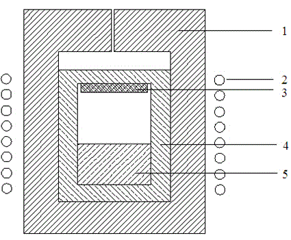
[0016] A 3-inch silicon carbide single crystal is grown in an induction heating PVT SiC single crystal furnace, and the specific steps are as follows:

[0017] (1) Place the SiC source powder on the lower part of the graphite crucible, place the SiC seed crystal on the upper part of the graphite crucible, the diameter of the SiC seed crystal is 3 inches, the growth surface is the carbon surface, and the growth direction is on-axis;

[0018] (2) Place the assembled graphite crucible in a high-frequency induction heating furnace;

[0019] (3) Use a molecular pump to evacuate the high-frequency induction heating furnace until the vacuum degree in the growth chamber reaches 5×10 -5 Below mbar;

[0020] (4) Introduce H into the growth chamber 2 and CH 4 Mixed gas, the ratio of the two is 1 : 1. The gas flow rate is 10mL / min, and the feeding time is 30min;

[0021] (5) After an interval of 30 minutes, inject the same amount of replacement gas as in step (4);

[0022] (6) The t...

Embodiment 2

[0025] The specific implementation steps of this example are different from those of Example 1: Repeat step (5) in Example 1 four times, that is, repeat the filling of replacement gas five times in total. The rest of the steps in this example are the same as in Example 1. I won’t go into details here. A 6H high-purity semi-insulating silicon carbide single crystal with a length greater than 3 cm and a diameter greater than 3 inches was obtained. The growth rate was greater than 0.6 mm / h. After cutting, grinding, and polishing, the resistivity was greater than 10 8 Ω·cm, the nitrogen content in the wafer was tested with a secondary ion mass spectrometer IMS-4F, and the nitrogen content was lower than 9×10 16 atom / cm 3 .


PUM

PropertyMeasurementUnit
electrical resistivityaaaaaaaaaa

Abstract

The invention relates to a method for rapidly growing a large-size high-purity semi-insulating silicon carbide single crystal. According to the method, on one hand, through multiple times of gas replacements conducted on a growing chamber, the insulation of the growing chamber and air is achieved, the nitrogen content in the single crystal is reduced, on the other hand, the rapid-growth of the silicon carbide single crystal is achieved through improving temperature gradient between source powder and a seed crystal in a silicon carbide single crystal growing system of a PVT method and / or reducing pressure of the growing chamber, and the crystal forms of the high-purity semi-insulating silicon carbide single crystal comprise a 4H, 6H, 3C and 15R or an arbitrary combined crystal form of the four crystal forms. The method for rapidly growing the large-size high-purity semi-insulating silicon carbide single crystal has the advantages that resistivity of the silicon carbide single crystal is improved, the growth speed of the silicon carbide single crystal can reach 0.5 mm / h-2 mm / h, the growth speed exceeds the conventional speed for multiple times, and the productive rate of the silicon carbide single crystal is further improved.

Description

technical field [0001] The invention relates to a method for growing a silicon carbide single crystal, in particular to a method for rapidly preparing a large-sized high-purity semi-insulating silicon carbide single crystal. Background technique [0002] Silicon carbide (SiC) material is the third-generation semiconductor material after silicon (Si) and gallium arsenide (GaAs), with wide band gap, high critical breakdown field strength, high electron saturation drift rate, high thermal conductivity, etc. It has become an ideal material for making high-temperature, high-frequency, high-power, and radiation-resistant devices. [0003] Semi-insulating silicon carbide single crystals include vanadium-doped semi-insulating and high-purity semi-insulating. When using a vanadium-doped silicon carbide substrate to make a device, vanadium can trap charges and cause an endogenous gate effect, which affects device performance. Therefore, it is best to use a high-purity semi-insulat...

Claims


Application Information

Patent Timeline
Patent Type & Authority Applications(China)
IPC IPC(8): C30B23/00C30B29/36
Inventor 窦瑛徐永宽孟大磊张皓张政徐所成
Owner CHINA ELECTRONICS TECH GRP NO 46 RES INST
Why Eureka
Try Eureka