
A kind of growth method of zno single crystal nano sheet

A growth method, single crystal nanotechnology, applied in the field of nanomaterial growth and preparation, can solve problems such as unfavorable integration of integrated circuit technology, and achieve the effects of high temperature resistance, physical and chemical properties, smooth structure surface, and weak binding force

Active Publication Date: 2017-06-16
WUHAN UNIV
View PDF4 Cites 0 Cited by
  • Summary
  • Abstract
  • Description
  • Claims
  • Application Information

AI Technical Summary

Problems solved by technology

However, the physical properties of ZnO determine that it is preferentially grown on the c-axis in most cases, so most of the growth of ZnO grows into a nanorod or columnar crystal structure, even if van der Waals epitaxy is introduced in the growth, Columnar crystals such as ZnO nanorods are still obtained [5,6], which is not conducive to integration in integrated circuit processes

Method used


Image

  • A kind of growth method of zno single crystal nano sheet
  • A kind of growth method of zno single crystal nano sheet
  • A kind of growth method of zno single crystal nano sheet

Examples


Embodiment 1

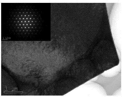
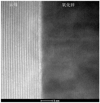
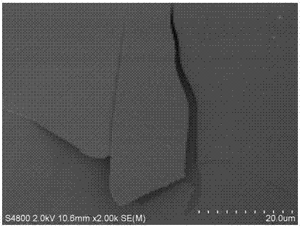
[0029] Fix the freshly cleaved fluorophlogopite substrate on a substrate holder and quickly load it into a pulsed laser deposition (PLD) vacuum chamber. The cavity air pressure is pumped to 10 -3 Below Pa, the substrate is heated to 550°C, and a 248nm pulse laser of 200mJ / pulse is used to focus on the ZnO ceramic target surface with a purity of 99.99%. The pulse frequency is 5Hz, and the deposition time is half an hour. 2 Anneal to room temperature at ambient. Depend on figure 1 The diffraction pattern of transmitted electron beam incident from ZnO [001] direction can be seen, and the diffraction pattern of ZnO single crystal can be clearly seen. The pattern is clear and regular, and the spots are complete. From figure 2 The high-resolution transmission electron micrographs of ZnO and mica show a good epitaxial relationship, and the interface is clear without amorphous transition layer. Depend on image 3 The scanning electron microscope shows that the size of single cr...

Embodiment 2

[0031] Fix the freshly cleaved fluorophlogopite substrate on the substrate holder and quickly put it into the PLD vacuum chamber. The cavity air pressure is pumped to 10 -3 Below Pa, heat the substrate to 450°C, use 200mJ / pulse 248nm pulsed laser to focus on the ZnO ceramic target surface with 99.99% purity, the pulse frequency is 5Hz, the deposition time is half an hour, and then in 3Pa O 2 Anneal to room temperature at ambient.

Embodiment 3

[0033] Fix the freshly cleaved fluorophlogopite substrate on the substrate holder and quickly put it into the PLD vacuum chamber. The cavity air pressure is pumped to 10 -3Below Pa, heat the substrate to 350°C, use 200mJ / pulse 248nm pulsed laser to focus on the ZnO ceramic target surface with 99.99% purity, the pulse frequency is 5Hz, the deposition time is half an hour, and then in 3Pa O 2 Anneal to room temperature at ambient.


PUM

PropertyMeasurementUnit
wavelengthaaaaaaaaaa
frequencyaaaaaaaaaa

Abstract

The invention discloses a growing method of a ZnO single-crystal nanosheet. According to the method, pulsed laser deposition is used for assisting in Van der Waals epitaxy, and the ZnO single-crystal nanosheet with the high covering rate grows on a stratified material substrate where Van der Waals force acts. High energy is adopted for assisting in Van der Waals deposition so that ZnO can be crystallized on the substrate, energy losses in the deposition process are reduced in high vacuum environment, the preferred growth direction of the ZnO can be changed in cooperation with proper deposition temperature and annealing temperature, so that the ZnO preferably grows in the surface, the traditional character of preferred growth in the ZnO (001) direction is changed, no columnar ZnO grows any more, a ZnO plane structure grows out, and traditional integrated circuit process integration and compatibility are facilitated. The binding force of the ZnO nanosheet growing through the method and the substrate is weak, and the ZnO nanosheet can be easily transferred to other substrates to process a semiconductor nanometer device.

Description

technical field [0001] The invention relates to a growth method of ZnO single-crystal nanosheets, belonging to the field of growth and preparation of nanometer materials. Background technique [0002] Zinc oxide (ZnO) is a II-VI group direct bandgap wide bandgap semiconductor material. Its band gap at room temperature is 3.37eV, and its exciton binding energy can reach 60meV, which is much higher than GaN's 25meV and room temperature thermal energy (26meV). It is very suitable for manufacturing light-emitting and optoelectronic devices that work stably at room temperature. However, the work of growing ZnO single crystal is indeed a challenging work. Due to the lattice mismatch, the growth of conventional ZnO single crystal nanomaterials usually requires a catalyst or a buffer layer to relieve the stress between the substrate and ZnO. At present, the epitaxial growth of ZnO on Si and sapphire substrates requires a suitable buffer layer to achieve. Although GaN has a small ...

Claims


Application Information

Patent Timeline
Patent Type & Authority Patents(China)
IPC IPC(8): C30B23/02C30B29/16C30B29/64B82Y40/00
Inventor 方国家李博睿
Owner WUHAN UNIV
Learn More