Preparation method of high temperature resistant packaging framework of silicon carbide diode

A technology of silicon carbide diodes and high temperature resistance, which is applied in semiconductor/solid-state device manufacturing, electrical components, electric solid-state devices, etc. It can solve the problems of reduced production efficiency and increased energy consumption, achieve high welding yield and reduce thermal resistance , Guarantee the effect of yield rate

Active Publication Date: 2015-12-02
淄博美林电子有限公司
View PDF5 Cites 13 Cited by
  • Summary
  • Abstract
  • Description
  • Claims
  • Application Information

AI Technical Summary

Problems solved by technology

However, this heating method will result in increased energy consumption and reduced production efficiency.

Method used


Image

  • Preparation method of high temperature resistant packaging framework of silicon carbide diode
  • Preparation method of high temperature resistant packaging framework of silicon carbide diode
  • Preparation method of high temperature resistant packaging framework of silicon carbide diode

Examples


Embodiment approach 1

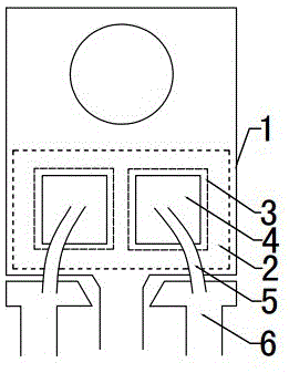
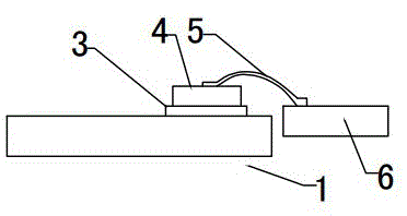
[0031] Other implementation mode 1: the basic structure and connection relationship are the same as the above-mentioned attached figure 1 , 2 As shown, the difference is that a nano-silver paste soldering layer 3 is provided on the crystal-bonding area 2, and a silicon carbide grain 4 and leads 5 connected to the left and right pins are welded on the nano-silver paste soldering layer 3.

Embodiment approach 2

[0032] Other implementation mode 2: the basic structure and connection relationship are the same as the above-mentioned attached figure 1 , 2 As shown, the difference is that the copper wires of the leads 5 are all replaced by aluminum wires.

[0033] Below through specific embodiment and in conjunction with appendix figure 1 The preparation method of a high-temperature-resistant packaging frame for a silicon carbide diode of the present invention will be further described, and the first embodiment is the best.

Embodiment 1

[0035] 1) Grain cutting: first paste the whole wafer on the UV film, use a laser cutting machine to cut the silicon carbide grain along the position of the grain cutting line, take it out and clean the surface of the silicon carbide grain 4 with pure water and dry it; The UV film used in the process has a high viscosity, 8000mN~10000mN, which is convenient for grain cutting and cleaning, and there will be no grain displacement or bruising;

[0036] 2) Screen printing: use a screen printing machine to evenly brush the nano-silver paste in the crystal-bonding area 2 on the copper frame to obtain the nano-silver paste welding layer 3;

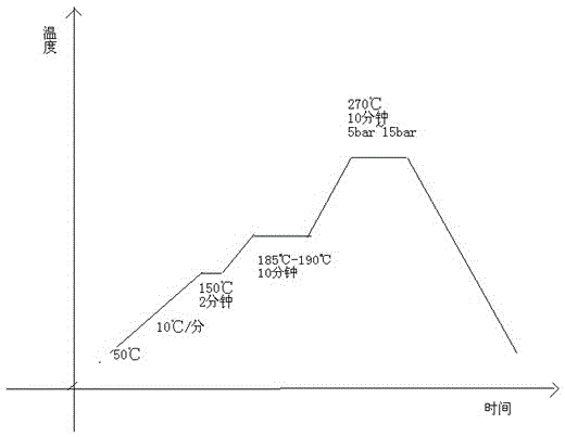
[0037] 3) Crystal bonding: use a crystal bonding machine to absorb silicon carbide grains 4 from the UV film irradiated by UV light and place them on the frame body 1; after the UV is illuminated, the viscosity becomes lower and drops to 1000mN, and the crystals are solidified to make crystals. It is easy to absorb when granulating, and it is not ...


PUM

PropertyMeasurementUnit
melting pointaaaaaaaaaa

Abstract

A preparation method of a high temperature resistant packaging framework of a silicon carbide diode belongs to the field of manufacture equipment for a semiconductor device. The preparation method is characterized by comprising the following low temperature sintering steps of: putting a framework main body (1) into a vacuum welding furnace, silicon carbide crystal grains (4) adhering to the framework main body by a nano-silver paste; vacuumizing the vacuum welding furnace to 50-55 mbar and then filling with nitrogen; heating the vacuum welding furnace at a speed of a speed of 10-12 DEG C / min to 150-155 DEG C and keeping the temperature for 2-4 min; and then continuously heating the vacuum welding furnace to 185-190 DEG C and keeping the temperature for 8-12 min; heating the vacuum welding furnace again to 270-275 DEG C; vacuumizing the vacuum welding furnace and filling with nitrogen to 5 bar-15 bar and keeping the pressure for 10-15 min to ensure a bonding strength; and then carrying out cooling, and finishing the welding of the silicon carbide crystal grains (4) and the framework main body (1). According to the invention, two weld zones (a cooling zone and a heating zone) are matched with special temperature curves, and a certain of pressure is added in a welding process. The welding time is shortened, and the production efficiency is improved.

Description

technical field [0001] The invention discloses a method for preparing a high-temperature-resistant packaging frame of a silicon carbide diode, which belongs to the field of semiconductor device manufacturing equipment. Background technique [0002] With the development of microelectronics technology, traditional silicon and gallium arsenide semiconductor materials have increasingly shown their deficiencies and limitations in terms of high temperature, high frequency, optoelectronics, high power and radiation resistance due to their own structure and characteristics. sex. As we all know, it is difficult for silicon devices to work normally when the temperature of the PN junction is higher than 150°C, especially when high operating temperature, high power, high frequency, and strong radiation environmental conditions coexist, silicon devices cannot be "competent". [0003] Silicon carbide has good characteristics such as large band gap, high breakdown electric field, high ele...

Claims


Application Information

Patent Timeline
Patent Type & Authority Applications(China)
IPC IPC(8): H01L21/60
CPCH01L24/05H01L24/13H01L24/81H01L2224/81H01L2224/83204H01L2224/8384H01L2224/85205H01L2224/29339H01L2224/32245H01L2224/45147H01L2224/48091H01L2224/48247H01L2224/48472H01L2224/73265H01L2924/00014H01L2924/00012H01L2924/00
Inventor 李安
Owner 淄博美林电子有限公司
Why Eureka
Try Eureka