Film solar cell and preparation method thereof

A solar cell and thin film technology, applied in circuits, photovoltaic power generation, electrical components, etc., can solve problems such as increasing the cost of batteries, and achieve the effects of avoiding recombination, improving photoelectric conversion efficiency, and increasing short-circuit current and open-circuit voltage.

Active Publication Date: 2015-12-09
PEKING UNIV SHENZHEN GRADUATE SCHOOL
View PDF4 Cites 21 Cited by
  • Summary
  • Abstract
  • Description
  • Claims
  • Application Information

AI Technical Summary

Problems solved by technology

At present, the main method to reduce surface carrier recombination is to form a very thick passivation layer, usually more than 50nm passivation layer, and then burn through the passivation layer during the electrode deposition process, so that the electrode Direct contact with the semiconductor layer, which has high requirements for the battery manufacturing process and electrode materials, thus increasing the cost of the battery

Method used


Image

  • Film solar cell and preparation method thereof
  • Film solar cell and preparation method thereof
  • Film solar cell and preparation method thereof

Examples


Embodiment 1

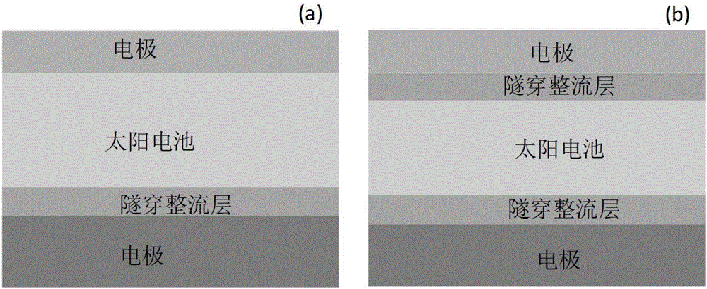
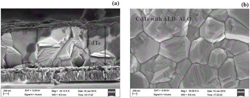
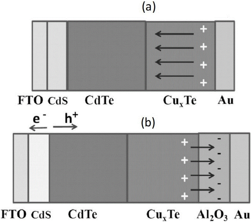
[0033] In this example, a cadmium telluride thin film solar cell was used for the experiment, and Al was formed on the surface of CdTe by atomic layer deposition 2 O 3 The tunneling rectification layer of this example is the tunneling rectification layer, which is disposed between the semiconductor layer and the back electrode layer.

[0034] The basic preparation process is as Image 6 As shown, a sputtering method is used to prepare a transparent front electrode layer FTO in sequence on a glass substrate, and the thickness can be 300 nm to 1 μm. In this example, a transparent electrode layer with a thickness of 500 nm is specifically prepared; then the n-type transition layer CdS is sputtered, and the thickness can be 100 -200nm. In this example, an n-type transition layer with a thickness of 145nm was specifically prepared, and a p-type light-absorbing layer CdTe film was prepared by vacuum evaporation deposition of CSS, and then CdCl was sequentially performed 2 Annealing, NP ...

Embodiment 2

[0038] This example uses cadmium telluride thin-film solar cells for testing. The difference from Example 1 is that this example will tunnel through the rectifier layer Al 2 O 3 The layer is provided between the semiconductor layer and the front electrode layer.

[0039] The transparent electrode layer FTO is prepared sequentially by sputtering method on the glass substrate. The thickness of this example can be 300nm~1μm. In this example, a transparent electrode layer with a thickness of 500nm is prepared; then Al is formed on the surface of the front electrode by atomic layer deposition 2 O 3 The tunneling rectifier layer of this example, the specific tunneling layer preparation process can refer to the specific process of Example 1, the thickness of the tunneling layer is 1nm; then the n-type transition layer CdS is sputtered, the thickness can be 100-200nm In this example, an n-type transition layer with a thickness of 145 nm was specifically prepared, and a p-type light-absorbi...

Embodiment 3

[0043] In this example, a copper indium gallium selenium thin film solar cell is used for the experiment. The physical vapor deposition method is mainly used to form cuprous oxide Cu on the back electrode of the copper indium gallium selenium thin film solar energy. 2 The O layer is the tunneling rectification layer of this example; the tunneling rectification layer is arranged between the semiconductor layer and the back electrode layer.

[0044] Sputtering on the glass substrate. The metal back electrode layer Mo is prepared by sputtering on the glass substrate in sequence. The thickness of this example can be 500nm~1μm. In this example, a metal electrode layer with a thickness of 1μm is prepared; the deposition temperature of the tunneling layer is 200℃. The background vacuum is 1.0×10 -3 Below Pa, pass argon Ar as the sputtering gas, and a small amount of oxygen as the reactive gas. (1) Under the action of the alternating electric field applied by the RF power supply to the sub...


PUM


Abstract

The invention discloses a film solar cell and a preparation method thereof. The film solar cell comprises a front electrode layer, a semiconductor layer, a back electrode layer and a tunneling rectification layer. The tunneling rectification layer of a single-layer or multi-layer structure is arranged between the front electrode layer and the semiconductor layer and/or between the semiconductor layer and the back electrode layer, and is made of at least one selected from metal oxide, metal nitride, metal sulfide and metal fluoride. The surface(s) of the front and/or back electrode layer are/is provided with the tunneling rectification layer, the tunneling rectification layer is used to carry out electron rectification, and thus, carrier combination is effectively avoided, the short-circuit current and open-circuit voltage of the solar cell are improved, and the photoelectric conversion efficiency is further improved.

Description

Technical field [0001] This application relates to the field of thin-film solar cells, in particular to a thin-film solar cell with an improved structure and a preparation method thereof. Background technique [0002] Thin-film solar cells are the main representative of the second-generation solar cells. Thin-film semiconductor materials are used as the light-absorbing layer, and the thickness is in the order of micrometers and sub-micrometers, which greatly reduces the consumption of materials. The growth process is simple, and it is convenient to make light and flexible devices. The price-performance ratio is superior, and the industrialization prospect is very good. However, thin-film semiconductor materials have many defects and serious surface carrier load. The photovoltaic conversion efficiency of the battery is currently only 10% to 20%, which is lower than that of traditional crystalline silicon solar cells. [0003] Based on the above reasons, how to reduce the recombinat...

Claims


Application Information

Patent Timeline
Patent Type & Authority Applications(China)
IPC IPC(8): H01L31/0352H01L31/18H01L51/42H01L51/48
CPCH01L31/035209H01L31/18H01L31/1828H10K30/151Y02E10/549Y02E10/543Y02P70/50
Inventor 潘锋梁军林钦贤苏彦涛张明建梅宗维杨晓杨
Owner PEKING UNIV SHENZHEN GRADUATE SCHOOL
Why Eureka
Try Eureka