Manufacturing method of back-channel-etching oxide thin-film transistor

An oxide thin film, back channel technology, applied in transistors, semiconductor/solid-state device manufacturing, semiconductor devices, etc., can solve the problems of high process temperature, corrosion, incompatible with flexible substrates, etc., to achieve high film formation rate, The effect of uniform composition

Active Publication Date: 2015-12-16
王磊 +1
View PDF4 Cites 12 Cited by
  • Summary
  • Abstract
  • Description
  • Claims
  • Application Information

AI Technical Summary

Problems solved by technology

Compared with DC sputtering, RF sputtering has disadvantages such as slow speed, constant adjustment and matching, poor process repeatability, uneven composition of multi-element films, and large RF radiation.
In addition, due to the high process temperature of the insulating layer and semiconductor active layer, it is difficult to be compatible with flexible substrates
[0004] On the other hand, when wet etching is used to etch the source and drain electrodes on the active layer, because the active la...

Method used


Image

  • Manufacturing method of back-channel-etching oxide thin-film transistor
  • Manufacturing method of back-channel-etching oxide thin-film transistor
  • Manufacturing method of back-channel-etching oxide thin-film transistor

Examples


Embodiment 1

[0041] A method for preparing a back-channel-etched oxide thin film transistor comprises the following preparation steps a, b, c, and d in sequence.

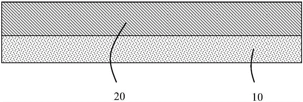
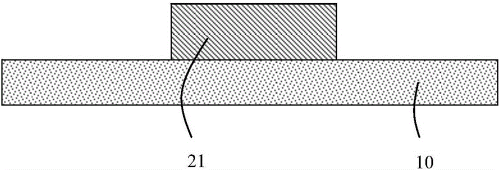
[0042] a. on the substrate 10, adopt the method of DC sputtering to prepare the first film layer 20, such as figure 2 As shown, the thickness is 100 to 1000 nm. Then the prepared first thin film layer 20 is patterned by wet etching method to obtain the first patterned thin film layer 21, the first patterned thin film layer 21 has a gate shape, such as image 3 shown.

[0043] The material of the first film layer 20 is a metal or an alloy that can be anodized to form an insulating oxide, such as aluminum, aluminum alloy, titanium, titanium alloy, tantalum or tantalum alloy, and the like.

[0044] The substrate 10 can be a glass substrate or a flexible substrate. When the substrate is a flexible substrate, it can be thin glass, polyethylene naphthalate (PEN), polyethylene terephthalate (PET), polyimide (PI) or metal foil, etc....

Embodiment 2

[0057] A method for preparing a back-channel-etched oxide thin film transistor comprises the following preparation steps a, b, c, and d in sequence.

[0058] a. on the substrate 10, adopt the method of DC sputtering to prepare the first film layer 20, such as figure 2 As shown, the material is metal tantalum with a thickness of 600nm. Then the prepared first thin film layer 20 is patterned by wet etching method to obtain the first patterned thin film layer 21, the first patterned thin film layer 21 has a gate shape, such as image 3 shown.

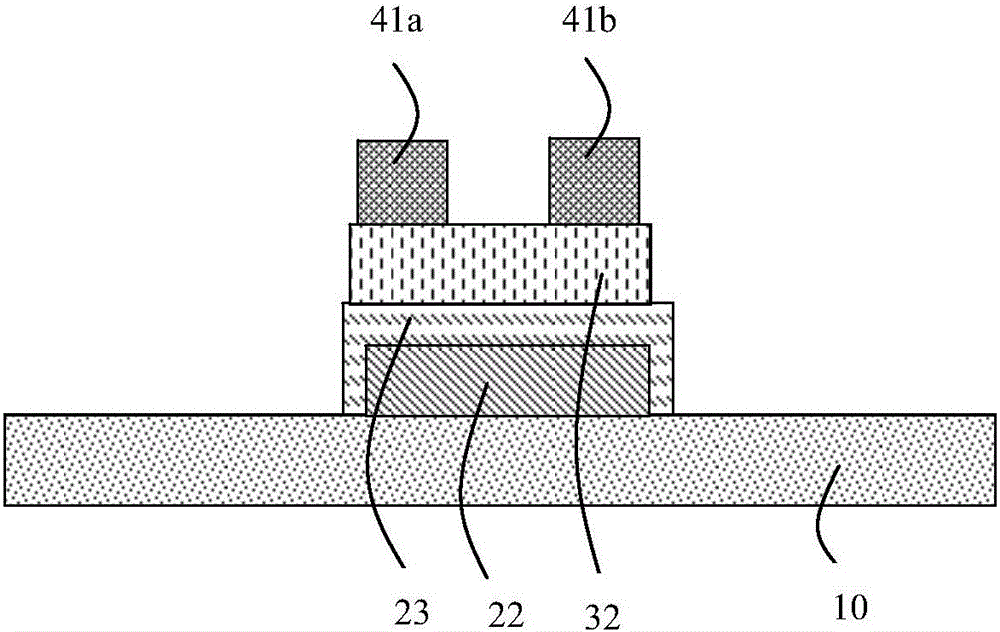
[0059] b. adopt the method for direct current sputtering to prepare the second film layer 30, such as Figure 4 As shown, the material is metallic tin with a thickness of 20nm. Then the prepared second thin film layer 30 is patterned by wet etching to obtain a second patterned thin film layer 31, and the second patterned thin film layer 31 has an active layer shape, such as Figure 5 shown.

[0060] c. adopt the method for direct cur...

Embodiment 3

[0069] A method for preparing a back-channel-etched oxide thin film transistor comprises the following preparation steps a, b, c, and d in sequence.

[0070] a. On the flexible PEN substrate 10 containing buffer layer, adopt the method for direct current sputtering to prepare the first film layer 20, as figure 2 As shown, the material is an aluminum neodymium alloy with a thickness of 300nm, and then the prepared first thin film layer 20 is patterned by wet etching to obtain the first patterned thin film layer 21, the first patterned thin film layer 21 have a gate shape such as image 3 shown.

[0071] b. adopt the method for direct current sputtering to prepare the second film layer 30, such as Figure 4 As shown, the material is a tin-zinc alloy with a thickness of 30nm. Then the prepared second thin film layer 30 is patterned by wet etching to obtain a second patterned thin film layer 31, and the second patterned thin film layer 31 has an active layer shape, such as F...


PUM

PropertyMeasurementUnit
Thicknessaaaaaaaaaa
Thicknessaaaaaaaaaa
Thicknessaaaaaaaaaa

Abstract

The invention discloses a manufacturing method of a back-channel-etching oxide thin-film transistor. The method sequentially comprises the following steps: (a) manufacturing a first thin-film layer on a substrate by a direct-current sputtering method and carrying out patterning; (b) manufacturing a second thin-film layer by the direct-current sputtering method and carrying out patterning; (c) manufacturing a third thin-film layer by the direct-current sputtering method and carrying out patterning as a source-drain electrode; and (d) putting the whole semi-finished product into electrochemical oxidation equipment for electrochemical oxidation, completely oxidizing a second patterned thin-film layer to form a second oxide layer, partially oxidizing a first patterned thin-film layer, and forming an oxide layer corresponding to a first thin-film layer material on the upper surface of the first patterned thin-film layer as a first oxide layer, wherein the unoxidized part of the first thin-film layer is taken as the residual first thin-film layer; the second oxide layer is taken as an active layer; the first oxide layer is taken as a gate insulation layer; and the residual first thin-film layer is taken as a gate. According to the manufacturing method, manufacturing is carried out at room temperature; radio-frequency sputtering is not needed; the manufacturing technique is simple; the production efficiency is high; and defects are few.

Description

technical field [0001] The invention relates to the technical field of semiconductors, in particular to a preparation method of an oxide thin film transistor. Background technique [0002] In recent years, the new flat panel display (FPD) industry has developed rapidly. Consumers' high demand for large-size, high-resolution flat-panel displays has stimulated the entire industry to continuously improve display technologies. The thin-film transistor (TFT) backplane technology, which is the core technology of the FPD industry, is also undergoing profound changes. Oxide TFTs not only feature high mobility and transparency to visible light, but also have excellent large-area uniformity. Therefore, the oxide TFT technology has attracted the attention of the industry since its birth. [0003] However, due to the low conductivity of the oxide semiconductor active layer, it is usually prepared by radio frequency sputtering. Compared with DC sputtering, RF sputtering has disadvant...

Claims


Application Information

Patent Timeline
IPC IPC(8): H01L21/34H01L29/786
CPCH01L29/7869H01L29/4908H01L29/66969H01L29/78696
Inventor 兰林锋彭俊彪
Owner 王磊
Why Eureka
Try Eureka