

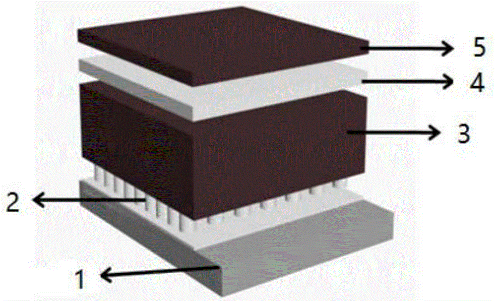
Self-driven photodetector based on ZnO nanorod/CH3NH3PbI3/MoO3 structure and preparation method thereof
A photodetector, nanorod technology, applied in nanotechnology, nanotechnology, nanotechnology and other directions for materials and surface science, can solve the problems of low saturation current and low defect density of diodes, and achieve controllable length, high Responsive, structurally novel effects
- Summary
- Abstract
- Description
- Claims
- Application Information
AI Technical Summary
Problems solved by technology
Method used
Image

Examples
Embodiment 1
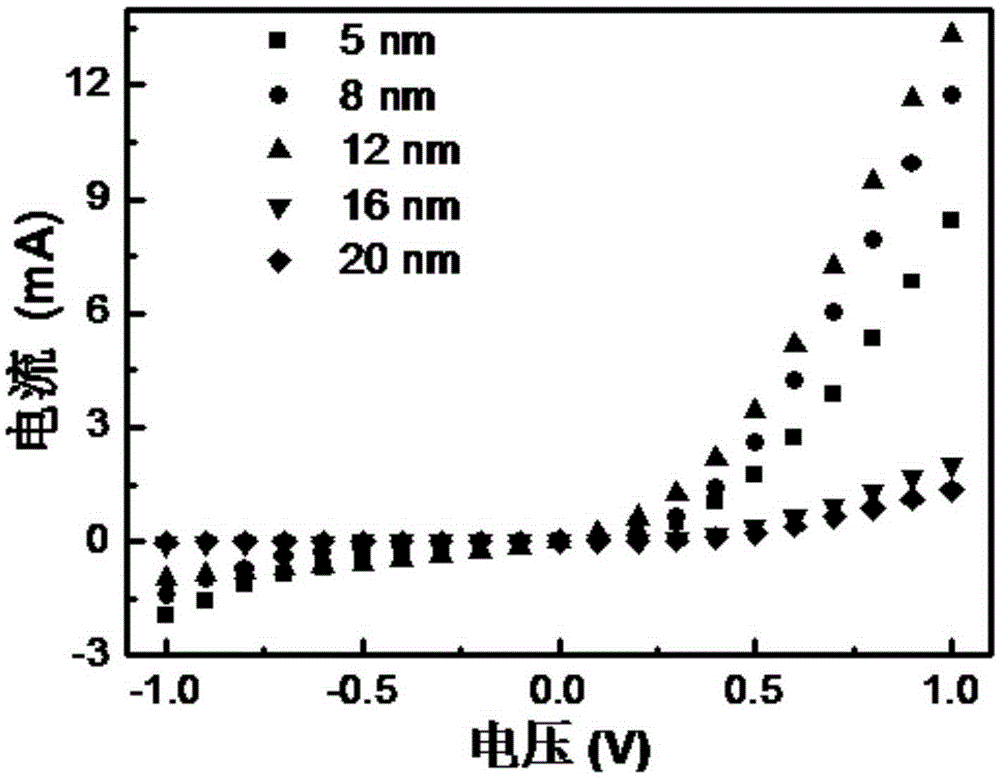
[0046] Example 1: 5nm thickness MoO 3 Preparation of the detector:
[0047] (1) Pretreatment of FTO: Cut the FTO glass sheet into square glass samples with an area of 2cm*2cm, then use deionized water, acetone, alcohol, and deionized water to carry out ultrasonic cleaning for 20 minutes, and the surface of the glass sheet Impurities are cleaned, and then cleaned with ultraviolet ozone (UV) for 15 minutes to remove organic matter attached to the surface.
[0048] (2) Preparation of ZnO seed layer: using methanol as solvent, prepare 5mmol / L zinc acetate (Zn(CH 3 COO) 2 ) solution, stirred for 5 minutes, and then started to spin-coat on the FTO glass sample at a rotation speed of 3000r / min for 15s, dried at 100°C for 15 minutes, and then transferred to a muffle furnace for annealing for 1h.
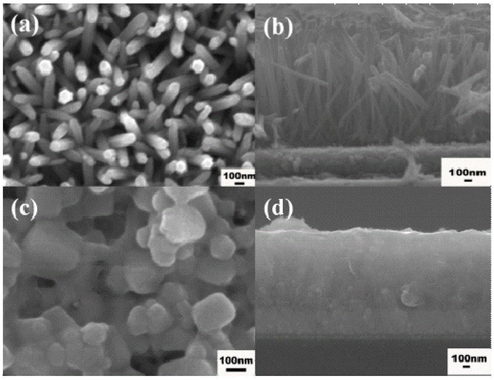
[0049] (3) Preparation of ZnO nanorods: grow ZnO nanorods in a water bath on the FTO glass sample with a ZnO seed layer, and the water bath solution composition is 50mmol / L zinc nitrate...
Embodiment 2
[0054] Example 2: 8nm thickness MoO 3 Preparation of the detector:
[0055] (1), (2), (3), (4) steps are identical with embodiment 1;
[0056] (5) Preparation of hole transport layer: using the method of evaporation, the semiconductor oxide MoO 3 Plated on the perovskite layer, keep 10 during evaporation -4 The vacuum degree, the evaporation rate is controlled at The thickness of vapor deposition was 8 nm.
[0057] (6) Preparation of the counter electrode: Au is used as the electrode material, and the evaporation method is adopted, and the evaporation rate is controlled at The thickness of evaporated Au is 40nm, and a complete photodetector can be fabricated.
[0058] The prepared ZnO nanorods and CH 3 NH 3 PB 3 X-ray diffraction (XRD) and scanning electron microscope (SEM) characterization were carried out respectively. The instrument used for X-ray diffraction analysis is D8Advance, and the measurement condition is 0.02° / step scan. The measurement voltage of the ...
Embodiment 3
[0059] Example 3: 12nm thickness MoO 3 Preparation of the detector:
[0060] (1), (2), (3), (4) steps are identical with embodiment 1;
[0061] (5) Preparation of hole transport layer: using the method of evaporation, the semiconductor oxide MoO 3 Plated on the perovskite layer, keep 10 during evaporation -4 The vacuum degree, the evaporation rate is controlled at The thickness of vapor deposition was 12 nm.
[0062](6) Preparation of the counter electrode: Au is used as the electrode material, and the evaporation method is adopted, and the evaporation rate is controlled at The thickness of evaporated Au is 40nm, and a complete photodetector can be fabricated.
[0063] The prepared ZnO nanorods and CH 3 NH 3 PB 3 X-ray diffraction (XRD) and scanning electron microscope (SEM) characterization were carried out respectively. The instrument used for X-ray diffraction analysis is D8Advance, and the measurement condition is 0.02° / step scan. The measurement voltage of the...
PUM
 Abstract
Description
Claims
Application Information