

High-polarization-intensity bismuth ferrite thick film material system and medium and low temperature preparation method
A polarization, bismuth ferrite technology, applied in the manufacture/assembly of semiconductor devices, piezoelectric/electrostrictive devices, electrical components, etc., can solve the problem of low withstand voltage, low polarization strength of bismuth ferrite materials, Easy leakage and other problems, to achieve the effect of low leakage, low cost and avoiding oxygen vacancies
- Summary
- Abstract
- Description
- Claims
- Application Information
AI Technical Summary
Problems solved by technology
Method used
Image

Examples
Embodiment 1
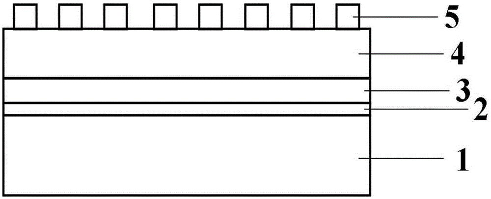
[0039] A method for preparing a bismuth ferrite thick film material with high polarization strength at medium and low temperatures, comprising the following steps:
[0040] (1) Treatment of the substrate
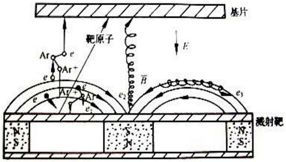
[0041] Cleaning and installation: using semiconductor silicon single crystal as the substrate, the substrate is ultrasonically cleaned with acetone and absolute ethanol in sequence, then rinsed with deionized water, dried with high-purity nitrogen, placed in the sample holder, and then the sample The holder is fixed on the sample holder in the vacuum chamber;
[0042] Vacuuming: Close the equipment chamber, pump the chamber with a mechanical pump to achieve a low vacuum, and then pump it with a molecular pump until the chamber pressure is 2×10 -4 Pa;
[0043] Heating: Introduce argon gas into the chamber, adjust the flow rate of argon gas to 39 sccm, and adjust the chamber pressure to 2.5 Pa at the same time, then heat the substrate to raise its temperature to 500°C.
[0...
Embodiment 2
[0051] The difference between this embodiment and Example 1 is that the substrate is heated to 450° C. in step (1), and other steps and parameters are the same as those in Example 1.
Embodiment 3
[0053] The difference between this embodiment and Example 1 is that in step (1), the substrate is heated to 475° C., and other steps and parameters are the same as in Example 1.
PUM
| Property | Measurement | Unit |
|---|---|---|
| Thickness | aaaaa | aaaaa |
| Thickness | aaaaa | aaaaa |
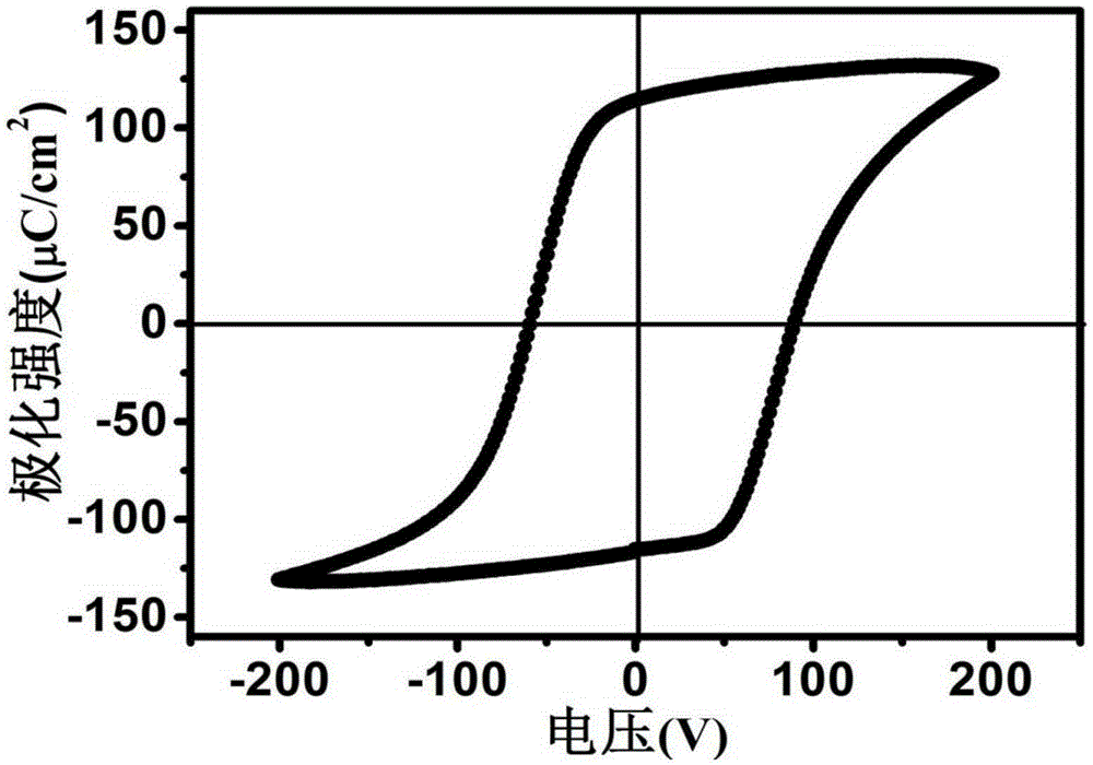
| Saturation polarization | aaaaa | aaaaa |
Abstract
Description
Claims
Application Information