

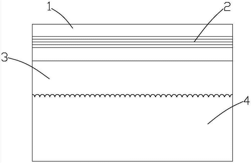
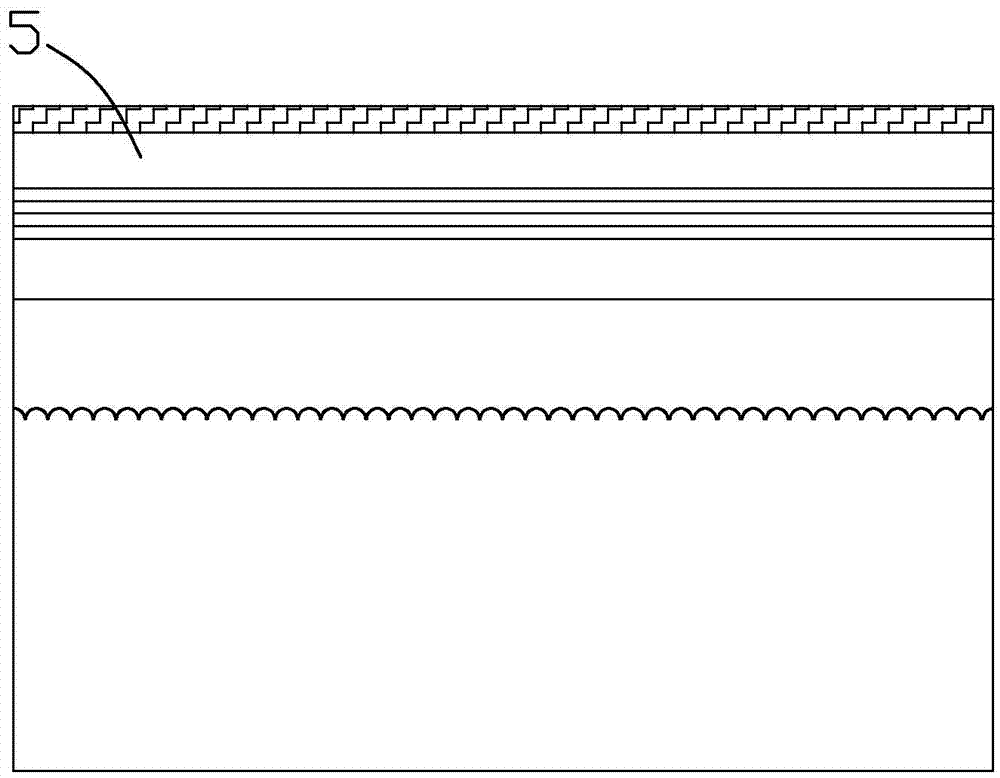
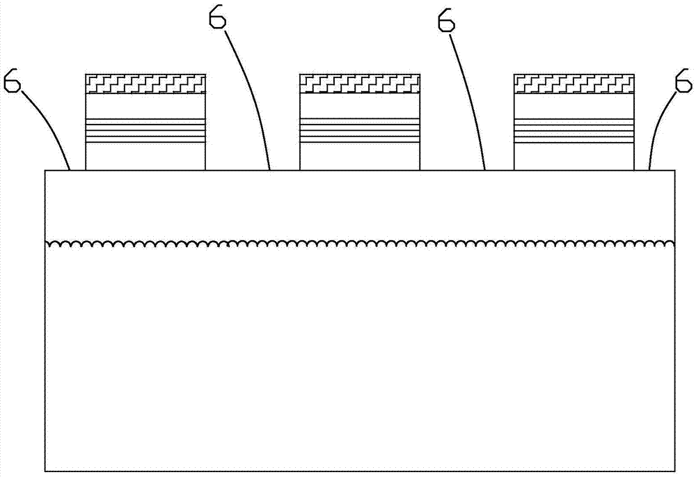
Inversed high-voltage light emitting diode (LED) chip electrode and chip fabrication method
A LED chip, high-voltage technology, applied in the direction of circuits, electrical components, electrical solid devices, etc., can solve the problems of motor blocking light-emitting drive life, uneven current diffusion, poor stability, etc., to reduce the current from the convergence effect, reduce light Decrease, enhance the effect of stability
- Summary
- Abstract
- Description
- Claims
- Application Information
AI Technical Summary
Problems solved by technology
Method used
Image

Examples
Embodiment 1
[0049] A method for manufacturing a flip-chip high-voltage LED chip as described above includes the following steps:
[0050] (1) Treat the substrate
[0051] Thinning, grinding and CMP polishing the back of the epitaxial wafer substrate grown on GaN to reduce its thickness from 430 μm to 180 μm, surface flatness (TTV) ≤ 50 μm, warpage (BOW) ≤ 50 μm, average roughness Degree S a ≤0.2nm;
[0052] (2) Clean the epitaxial layer
[0053] Pickle the light gallium nitride epitaxial wafer on which the chip is made, and wash it with aqua regia (HCl: HNO 3 =3:1) Imaging and etching for 30 minutes, mainly cleaning and removing metal pollutants on the wafer surface; 2 SO 4 :H 2 o 2 = 1:4 wash at room temperature for 5 minutes, mainly to remove surface organic contamination; then use HF:H 2 O (DI, ultrapure water) = 1: 1 to remove the oxide layer on the wafer surface, and finally rinse and dry with deionized water;
[0054] (3) P-type gallium nitride surface roughening
[0055] ...
Embodiment 2
[0070] A method for manufacturing a flip-chip high-voltage LED chip as described above includes the following steps:
[0071] (1) Treat the substrate
[0072] Thinning, grinding and CMP polishing the back of the epitaxial wafer substrate grown on GaN to reduce its thickness from 430 μm to 180 μm, surface flatness (TTV) ≤ 50 μm, warpage (BOW) ≤ 50 μm, average roughness Degree S a ≤0.2nm;
[0073] (2) Clean the epitaxial layer
[0074] Pickle the light gallium nitride epitaxial wafer on which the chip is made, and wash it with aqua regia (HCl: HNO 3 =3:1) Imaging and etching for 30 minutes, mainly cleaning and removing metal pollutants on the wafer surface; 2 SO 4 :H 2 o 2 = 1:4 wash at room temperature for 5 minutes, mainly to remove surface organic contamination; then use HF:H 2 O (DI, ultrapure water) = 1: 1 to remove the oxide layer on the wafer surface, and finally rinse and dry with deionized water;
[0075] (3) Surface roughening of P-type gallium nitride
[007...
PUM
| Property | Measurement | Unit |
|---|---|---|
| Etching depth | aaaaa | aaaaa |
| Thickness | aaaaa | aaaaa |
| Thickness | aaaaa | aaaaa |
Abstract
Description
Claims
Application Information