

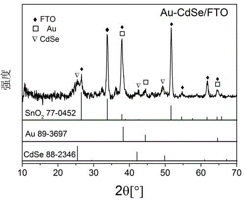
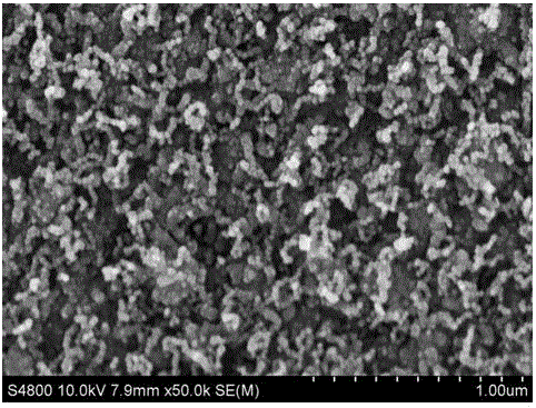
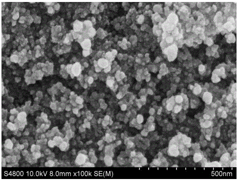
Method for spontaneously growing Au nanometer particles on electro-deposited CdSe film
A nanoparticle and spontaneous growth technology, applied in the field of nanomaterials and electrochemistry, can solve the problems of difficult large-scale industrial production, cumbersome preparation steps, and many solvents used, and achieve easy large-scale promotion, simple preparation process, and thin film adhesion. strong effect
- Summary
- Abstract
- Description
- Claims
- Application Information
AI Technical Summary
Problems solved by technology
Method used
Image

Examples
Embodiment 1
[0019] (1) The electrodes were ultrasonically cleaned with analytical pure acetone, analytical pure ethanol and secondary water for 3 minutes respectively, and after drying in the air, the conductive side was measured with a multimeter, and it was used as a base electrode for later use.
[0020] (2) Measure 6 mL of divalent cadmium salt solution with a concentration of 0.05 mol / L in a clean small beaker, and add 1 mL of SeO with a concentration of 0.01 mol / L in six times under magnetic stirring. 2 Aqueous solution to prepare electrodeposited CdSe thin film base solution.
[0021] (3) Construct a three-electrode system in the electrodeposited CdSe thin film base solution prepared in step (2), wherein the base electrode prepared in step (1) is used as a working electrode, Ag / AgCl is used as a reference electrode, and Pt is used as an auxiliary electrode , using cyclic voltammetry for electrodeposition, the scanning range is -1.1~0V, the scanning speed is 0.05V / s, and the number ...
Embodiment 2
[0028] (1) The electrodes were ultrasonically cleaned with analytical pure acetone, analytical pure ethanol and secondary water for 3 minutes respectively, and after drying in the air, the conductive side was measured with a multimeter, and it was used as a base electrode for later use.
[0029] (2) Measure 6mL of divalent cadmium salt solution with a concentration of 0.1mol / L in a clean small beaker, and add 1mL of SeO with a concentration of 0.05mol / L in six times under magnetic stirring. 2 Aqueous solution to prepare electrodeposited CdSe thin film base solution.
[0030] (3) Construct a three-electrode system in the electrodeposited CdSe thin film base solution prepared in step (2), wherein the base electrode prepared in step (1) is used as a working electrode, Ag / AgCl is used as a reference electrode, and Pt is used as an auxiliary electrode , using cyclic voltammetry for electrodeposition, the scanning range is -1.1~0V, the scanning speed is 0.05V / s, and the number of sc...
Embodiment 3
[0036] (1) The electrodes were ultrasonically cleaned with analytical pure acetone, analytical pure ethanol and secondary water for 3 minutes respectively, and after drying in the air, the conductive side was measured with a multimeter, and it was used as a base electrode for later use.
[0037] (2) Measure 6 mL of divalent cadmium salt solution with a concentration of 0.15 mol / L in a clean small beaker, and add 1 mL of SeO with a concentration of 0.1 mol / L in six times under magnetic stirring. 2 Aqueous solution to prepare electrodeposited CdSe thin film base solution.
[0038] (3) Construct a three-electrode system in the electrodeposited CdSe thin film base solution prepared in step (2), wherein the base electrode prepared in step (1) is used as a working electrode, Ag / AgCl is used as a reference electrode, and Pt is used as an auxiliary electrode , using cyclic voltammetry for electrodeposition, the scanning range is -1.1~0V, the scanning speed is 0.05V / s, and the number o...
PUM
| Property | Measurement | Unit |
|---|---|---|
| Concentration | aaaaa | aaaaa |
Abstract
Description
Claims
Application Information