LED filament preparation method
A technology of LED filaments and LED chips, which is applied in the direction of electrical components, electric solid devices, circuits, etc., can solve the problems of complex manufacturing process, inconvenience of large-angle light emission, and unsightly appearance, and achieve long service life, easy promotion and application, Good bonding strength
- Summary
- Abstract
- Description
- Claims
- Application Information
AI Technical Summary
Problems solved by technology
Method used
Image

Examples
Embodiment 1
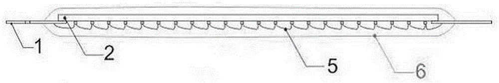
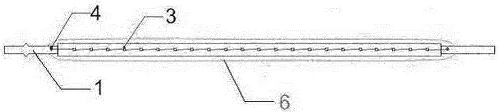
[0020] The embodiment is basically as attached figure 1 , 2 As shown: the preparation method of the LED filament in this embodiment includes a strip-shaped transparent substrate 2, a metal bracket 1 fixed on both ends of the transparent substrate, a plurality of blue LED chips 3 are fixed on the transparent substrate, and the plurality of blue LED chips form at least one row through For the LED strings on the transparent substrate, the blue LED chips of each LED string are connected in series by wires; the blue LED chips located at both ends 4 of the transparent substrate are respectively connected to the support by wires 5;
[0021] The outside of the transparent substrate is also wrapped with a red phosphor layer 6 , and the red phosphor layer is formed by mixing red phosphor and a binder.
[0022] When in use, connect the metal brackets at both ends of the transparent substrate to the positive and negative poles of the power supply, and the two metal brackets are electrica...
Embodiment 2
[0033]The bonding agent also includes the following raw materials prepared in parts by weight: 72 parts of epoxy resin, 18-22 parts of polyphenylene ether powder, 4 parts of methylphenyl silicone oil, 0.2-0.4 of nano-zinc sulfide, with a mass concentration of 30 -40% nano ceramic powder transparent liquid 6-8, nano titanium dioxide 4-5, benzoyl peroxide 0.1-0.2, maleic anhydride 0.4-0.5, silane coupling agent 0.1-0.2, chloroform antioxidant 0.01-0.02 parts, curing agent 20-25 parts.
[0034] The preparation method is:
[0035] (1) Pre-irradiate the polyphenylene ether powder. The irradiation conditions are: use an electron accelerator as the irradiation source, and use β-rays to irradiate under normal temperature, normal pressure, and air atmosphere. The pre-irradiation dose range 20kGy, to obtain pre-irradiated polyphenylene ether material;
[0036] (2) Put the pre-irradiated polyphenylene ether material, maleic anhydride, silane coupling agent, nano-titanium dioxide, benzo...
Embodiment 3
[0043] The preparation method of described methyl phenyl silicone oil is as follows:
[0044] The components weighed in parts by weight are: 30 parts of methylphenyl mixed rings, 30 parts of octamethylcyclotetrasiloxane, 20 parts of tetramethylcyclotetrasiloxane, tetramethyldivinyl disiloxane 10 parts of oxane, 5 parts of potassium hydroxide silicon alkoxide, 5 parts of organic silicon phosphate.
[0045] Then, prepare methylphenyl silicone oil: (1) add methylphenyl mixed ring body, octamethylcyclotetrasiloxane, tetramethylcyclotetrasiloxane, tetramethyldivinyldisiloxane In the reactor, dehydrate for 2 hours at a temperature of 60°C and a pressure of -0.1MPa; (2) raise the temperature of the dehydrated mixture to 180°C, add potassium hydroxide silicon alkoxide catalyst, and dehydrate at a temperature of 185°C Equilibrium reaction for 8 hours; (3) After the reaction is completed, add organosilicon phosphate in proportion to the reactor for neutralization for 2.5 hours, then ra...
PUM
 Abstract
Description
Claims
Application Information
 - R&D
- Intellectual Property
- Life Sciences
- Materials
- Tech Scout
- Unparalleled Data Quality
- Higher Quality Content
- 60% Fewer Hallucinations
Browse by: Latest US Patents, China's latest patents, Technical Efficacy Thesaurus, Application Domain, Technology Topic, Popular Technical Reports.
© 2025 PatSnap. All rights reserved.Legal|Privacy policy|Modern Slavery Act Transparency Statement|Sitemap|About US| Contact US: help@patsnap.com