3D branch semiconductor nano heterojunction photoelectrode material and preparing method thereof

A heterojunction, photoelectrode technology, applied in electrodes, nanotechnology, nanotechnology, etc., can solve problems such as limiting large-scale applications, and achieve the effects of reducing compounding, improving efficiency, and increasing specific surface area.

Active Publication Date: 2016-05-11
SUZHOU UNIV
View PDF5 Cites 11 Cited by
  • Summary
  • Abstract
  • Description
  • Claims
  • Application Information

AI Technical Summary

Problems solved by technology

[0002] The depletion of fossil fuels has become a well-known problem since the development of human beings, and various corresponding methods to improve this crisis have attracted widespread attention. Solar energy, as an inexhaustible and inexhaustible Energy is a powerful resource to solve this problem, and the corresponding solar cell is a device that converts solar energy into chemical energy, but the biggest shortcoming of this device is that it only works when there is sun Only when it can work, can it create energy that can be used by human beings. This inevitable defect will obviously limit its large-scale application. It is undoubtedly the most effective way to solve this problem by storing the produced chemical energy as fuel. also the most feasible way

Method used


Image

  • 3D branch semiconductor nano heterojunction photoelectrode material and preparing method thereof
  • 3D branch semiconductor nano heterojunction photoelectrode material and preparing method thereof

Examples


Embodiment 1

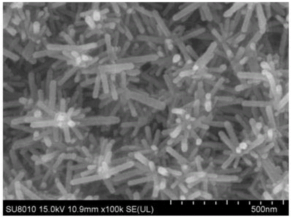
[0034] The FTO (fluorine-doped tin oxide) conductive substrate was ultrasonically cleaned in alcohol, acetone and deionized water for 15 minutes each. Dissolve 0.1245g of copper acetate monohydrate evenly in 62.5mL of alcohol to make a seed layer solution. The prepared seed layer solution was measured with a 1mL pipette gun and evenly spin-coated on the conductive substrate several times with a coater, and then the spin-coated sample was sintered at 400°C for 2 hours. Prepare an aqueous solution uniformly mixed with 25mmol / L methylenetetramine and 25mmol / L copper nitrate trihydrate, measure 10mL of the aqueous solution and place it in a polytetrafluoroethylene-lined autoclave with a volume of 20mL, and place the treated conductive substrate Conductive side down, placed in the autoclave lining at a certain angle, the autoclave was heated to 80 ° C and kept for 6 hours, after the reaction was completed, the autoclave was cooled to room temperature and the samples were taken out,...

Embodiment 2

[0036]The FTO (fluorine-doped tin oxide) conductive substrate was ultrasonically cleaned in alcohol, acetone and deionized water for 15 minutes each. Dissolve 0.1245g of copper acetate monohydrate evenly in 62.5mL of alcohol to make a seed layer solution. The prepared seed layer solution was measured with a 1mL pipette gun and evenly spin-coated on the conductive substrate several times with a coater, and then the spin-coated sample was sintered at 400°C for 2 hours. Prepare an aqueous solution uniformly mixed with 25mmol / L hexamethylenetetramine and 25mmol / L copper nitrate trihydrate, measure 10mL of the aqueous solution and place it in a polytetrafluoroethylene-lined autoclave with a volume of 20mL, and place the treated conductive The conductive surface of the substrate is facing down, placed in the autoclave lining at a certain angle, the autoclave is heated to 80 °C and kept for 6 hours, after the reaction is completed, the samples are taken out after the autoclave is coo...

Embodiment 3

[0038] The FTO (fluorine-doped tin oxide) conductive substrate was ultrasonically cleaned in alcohol, acetone and deionized water for 15 minutes each. Dissolve 0.1245g of copper acetate monohydrate evenly in 62.5mL of alcohol to make a seed layer solution. The prepared seed layer solution was measured with a 1 mL pipette gun and evenly spin-coated on the conductive substrate several times with a homogenizer, and then the spin-coated sample was sintered at 400 °C for 2 hours. Prepare an aqueous solution uniformly mixed with 25mmol / L hexamethylenetetramine and 25mmol / L copper nitrate trihydrate, measure 10mL of the aqueous solution and place it in a polytetrafluoroethylene-lined autoclave with a volume of 20mL, and place the treated conductive The conductive surface of the substrate is facing down, placed in the autoclave lining at a certain angle, the autoclave is heated to 80 °C and kept for 6 hours, after the reaction is completed, the samples are taken out after the autoclav...


PUM


Abstract

The invention discloses a 3D branch semiconductor nano heterojunction photoelectrode material and a preparing method thereof. The heterojunction photoelectrode material is compounded by CuO and ZnO, and is in a 3D branch structure. In the method, ZnO branch nanobars are synthesized on the CuO nanobars, a branch nano structure is realized, and a 3D branch semiconductor nano heterojunction photocathode is prepared, which effectively increases absorption for sunlight, thereby accelerating effective separation of an electron hole pair, further reducing composition thereof, promoting charge transmission, optimizing photoelectric conversion efficiency of a traditional single semiconductor electrode, and improving photolysis efficiency of water; in addition, the material has advantages of environment friendliness and low cost, and has good application prospect.

Description

technical field [0001] The invention relates to a photoelectrochemical battery electrode material and a preparation method thereof, in particular to a 3D branched semiconductor nano-heterojunction photoelectrode material and a preparation method thereof. Background technique [0002] The depletion of fossil fuels has become a well-known problem since the development of human beings, and various corresponding methods to improve this crisis have attracted widespread attention. Solar energy, as an inexhaustible and inexhaustible Energy is a powerful resource to solve this problem, and the corresponding solar cell is a device that converts solar energy into chemical energy, but the biggest shortcoming of this device is that it only works when there is sun Only when it can work, can it create energy that can be used by human beings. This inevitable defect will obviously limit its large-scale application. It is undoubtedly the most effective way to solve this problem by storing th...

Claims


Application Information

Patent Timeline
Patent Type & Authority Applications(China)
IPC IPC(8): C25B11/02C25B11/04C25B1/04B82Y30/00B82Y40/00
CPCB82Y30/00B82Y40/00C25B1/04C25B11/02C25B11/04Y02E60/36
Inventor 李亮田维武芳丽
Owner SUZHOU UNIV
Why Eureka
Try Eureka