High-efficiency quantum dot light emitting diode with self-assembly polymer hole transmission layer structure
A technology of quantum dot luminescence and hole transport layer, which is applied in the field of high-efficiency quantum dot light-emitting diodes with a three-layer structure of self-assembled polymer hole buffer transport layer, can solve problems affecting device life and load power, and achieve energy efficiency and high efficiency. Efficiency, the effect of simple preparation method
- Summary
- Abstract
- Description
- Claims
- Application Information
AI Technical Summary
Problems solved by technology
Method used
Image
Examples
Embodiment 1
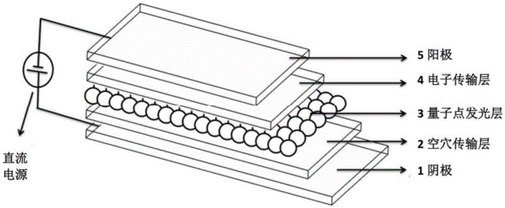
[0024] High-efficiency quantum dot light-emitting diodes with forward self-assembled polymer hole layers, such as figure 1 As shown, it includes a cathode 1, a hole transport layer 2, a quantum dot light-emitting layer 3, an electron transport layer 4 and an anode electrode 5 formed on the substrate. layer, electron transport layer and anode, wherein the hole transport layer is 10nm thick, the quantum dot light-emitting layer is 20nm thick, and the electron transport layer is 30nm thick.
[0025] The preparation method of the high-efficiency quantum dot light-emitting diode of the above-mentioned forward self-assembled polymer hole layer comprises the following steps:
[0026] (1) Preparation of hole transport layer perfluoroionomer PFIs doped poly3,4-ethylenedioxythiophene monomer PEDOT:PSS on transparent conductive glass substrate by inkjet method, mass fraction of perfluoroionomer PFIs 10%, and sintered under nitrogen atmosphere for 20 minutes, the sintering temperature is...
Embodiment 2
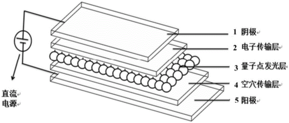
[0031] Efficient quantum dot light-emitting diodes with inverted self-assembled polymer hole layers, such as figure 2 As shown, it includes an anode 1, an electron transport layer 2, a quantum dot light-emitting layer 3, a hole transport layer 4 and a cathode electrode 5 formed on the substrate. , a hole transport layer and a cathode, wherein the thickness of the electron transport layer is 50nm, the thickness of the quantum dot light-emitting layer is 30nm, and the thickness of the hole transport layer is 20nm.
[0032] The preparation method of the high-efficiency quantum dot light-emitting diode of the above-mentioned reverse self-assembled polymer hole layer comprises the following steps:
[0033] (1) Calcium-doped TiO 2 The nanoparticle layer is prepared on the anode electrode Al, and the inorganic nanoparticle light-emitting layer is sintered in oxygen for 20 minutes at a sintering temperature of 200°C.
[0034] (2) Preparation of quantum dots: The quantum dot layer p...
Embodiment 3
[0038] High-efficiency quantum dot light-emitting diodes with forward self-assembled polymer hole layers, such as figure 1 As shown, it includes a cathode 1, a hole transport layer 2, a quantum dot light-emitting layer 3, an electron transport layer 4 and an anode electrode 5 formed on the substrate. layer, electron transport layer and anode, wherein the hole transport layer is 30nm thick, the quantum dot luminescent layer is 40nm thick, and the electron transport layer is 70nm thick.
[0039] The preparation method of the high-efficiency quantum dot light-emitting diode of the above-mentioned forward self-assembled polymer hole layer comprises the following steps:
[0040] (1) The hole transport layer was prepared by inkjet method on the transparent conductive glass substrate. The mass fraction of vinyl PPV was 5%, and the hole transport layer was prepared, and sintered in a nitrogen environment for 20 minutes, and the sintering temperature was 150 degrees.
[0041] (2) Prepa...
PUM
| Property | Measurement | Unit |
|---|---|---|
| Diameter | aaaaa | aaaaa |
| Size | aaaaa | aaaaa |
Abstract
Description
Claims
Application Information

