Microscopic imaging device and method for measuring microstructure defects on surface of semiconductor material

A technology of microscopic imaging and microstructure, which is applied in the direction of measuring devices, optical testing of defects/defects, and analysis of materials, can solve the problems of complex testing process, large measurement error, and expensive testing cost, and achieve accurate test results and accurate preparation process. simple effect

Inactive Publication Date: 2016-06-08
INST OF SEMICONDUCTORS - CHINESE ACAD OF SCI
View PDF6 Cites 14 Cited by
  • Summary
  • Abstract
  • Description
  • Claims
  • Application Information

AI Technical Summary

Problems solved by technology

[0006] The purpose of the present invention is to provide a microscopic imaging device and method for measuring microstructural defects on the surface of semiconductor materials, so as to solve the problem of large measurement errors in the current characterization methods for microstructural defects in materials, the inability to directly characterize the microstructural defects of materials, and the complicated testing process And the cost of testing is expensive, so as to achieve the purpose of no damage to the material, convenient and efficient, and simple operation.

Method used


Image

  • Microscopic imaging device and method for measuring microstructure defects on surface of semiconductor material
  • Microscopic imaging device and method for measuring microstructure defects on surface of semiconductor material
  • Microscopic imaging device and method for measuring microstructure defects on surface of semiconductor material

Examples


Embodiment Construction

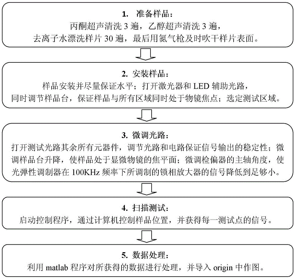
[0031] In order to make the object, technical solution and advantages of the present invention clearer, the present invention will be further described in detail below in conjunction with specific embodiments and with reference to the accompanying drawings.

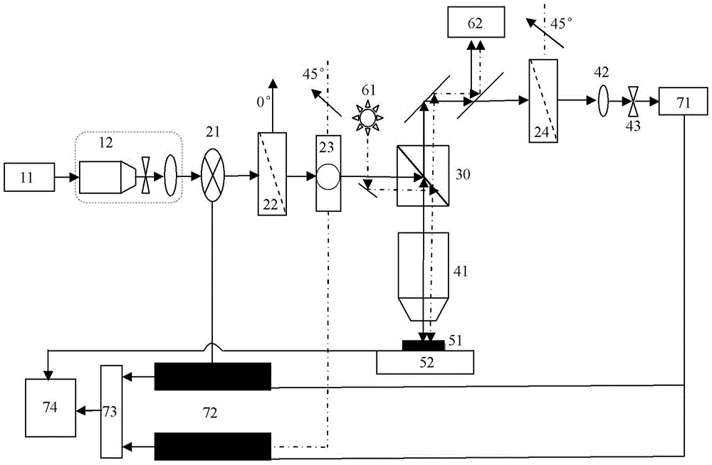
[0032] Such as figure 1 As shown, the present invention provides a device for measuring the microscopic imaging of microstructure defects on the surface of semiconductor materials. The testing device mainly includes: a light source 10, a polarization modulation reflective differential system 20, a beam splitting prism 30, a confocal microscope system 40, a scanning platform 50, a signal acquisition system 70, and an auxiliary optical path 60 for assisting in focusing and determining Sample test location.

[0033] Wherein, the light source 10 includes a single-wavelength laser 11 and a spatial filter 12, which is a single-wavelength laser to generate laser light, which is used to provide a high-quality parallel and unifor...


PUM


Abstract

The invention discloses a microscopic imaging device and method for measuring microstructure defects on a surface of a semiconductor material. The testing device comprises a light source, a polarization modulation reflection difference system, a beam splitter prism, a scanning platform, a co-focusing microscopic system and a signal acquisition system. According to a photo-elastic effect principle and a crystal defect theory, although the microstructure defects on the surface of the semiconductor material have very small sizes, a very large strain distribution field relative to the microstructure defects is formed around the microstructure defects and the strain distribution field can generate an optical reflection anisotropic signal; the testing method can be used for measuring the optical reflection anisotropic signal of each measuring point around the microstructure defects so that an optical reflection anisotropic microscopic imaging pattern, which is close to the microstructure defects, related with the strain field and changed along with a space position, can be directly obtained, and furthermore, information including varieties, density, strain distribution and the like of the defects is obtained. With regard to characterization of the microstructure defects of the material, the microscopic imaging device and method, disclosed by the invention, have the advantages of simplicity and efficiency for operation, no damages, strong portability and the like.

Description

technical field [0001] The invention relates to the technical field of semiconductor material testing, in particular to a microscopic imaging device and method for measuring surface microstructure defects of semiconductor materials. Background technique [0002] The third-generation semiconductor materials represented by gallium nitride (GaN), silicon carbide (SiC) and zinc oxide (ZnO) have large band gap, high breakdown electric field, high thermal conductivity, high electron saturation rate and anti- The advantages of strong radiation ability are more suitable for the production of high-temperature, high-frequency, radiation-resistant and high-power devices. It is also the "core" of solid-state light sources and power electronic microwave radio frequency devices, and is becoming a new strategic highland for the global semiconductor industry. [0003] In the past 20 years, crystal growth scientists in various countries have been working hard to grow large-size, high-quality...

Claims


Application Information

Patent Timeline
Patent Type & Authority Applications(China)
IPC IPC(8): G01N21/95
CPCG01N21/9501
Inventor 黄威陈涌海刘雨高寒松李远邬庆
Owner INST OF SEMICONDUCTORS - CHINESE ACAD OF SCI
Why Eureka
Try Eureka