Method for efficiently electroplating and filling silicon-based TSV

A silicon-based, high-efficiency technology, applied in the manufacture of circuits, electrical components, semiconductors/solid-state devices, etc., can solve the constraints on the application and development of 3D-TSV packaging technology, affect the thermomechanical stability and electrical properties of TSV, and the end of deep holes The difficulty of controlling the plating rate is high, achieving the effects of high thermomechanical stability, good electrical conductivity, and good bonding force

Active Publication Date: 2016-06-15
SHANGHAI JIAO TONG UNIV
View PDF4 Cites 8 Cited by
  • Summary
  • Abstract
  • Description
  • Claims
  • Application Information

AI Technical Summary

Problems solved by technology

These processes are still immature, which restricts the application and development of 3D-TSV packaging technology
[0003] The thermal mechanical reliability and electrical performance reliability of 3D-TSV packaging technology is a huge challenge for this process technology to achieve mass production
Residual stress and thermal stress between the interface between Cu-TSV and TSV-pad naturally exist, and TSV filling is blin

Method used


Image

  • Method for efficiently electroplating and filling silicon-based TSV
  • Method for efficiently electroplating and filling silicon-based TSV

Examples


Embodiment 1

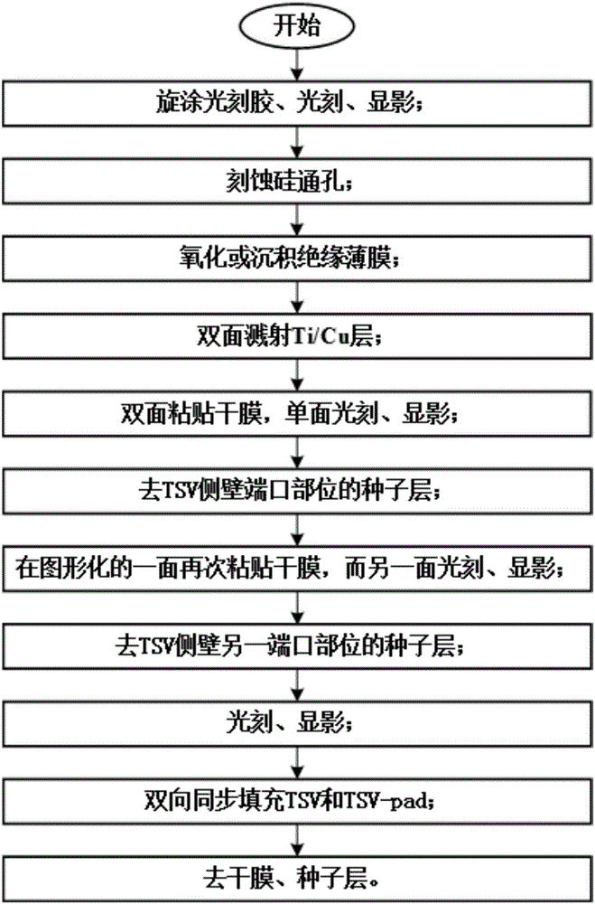
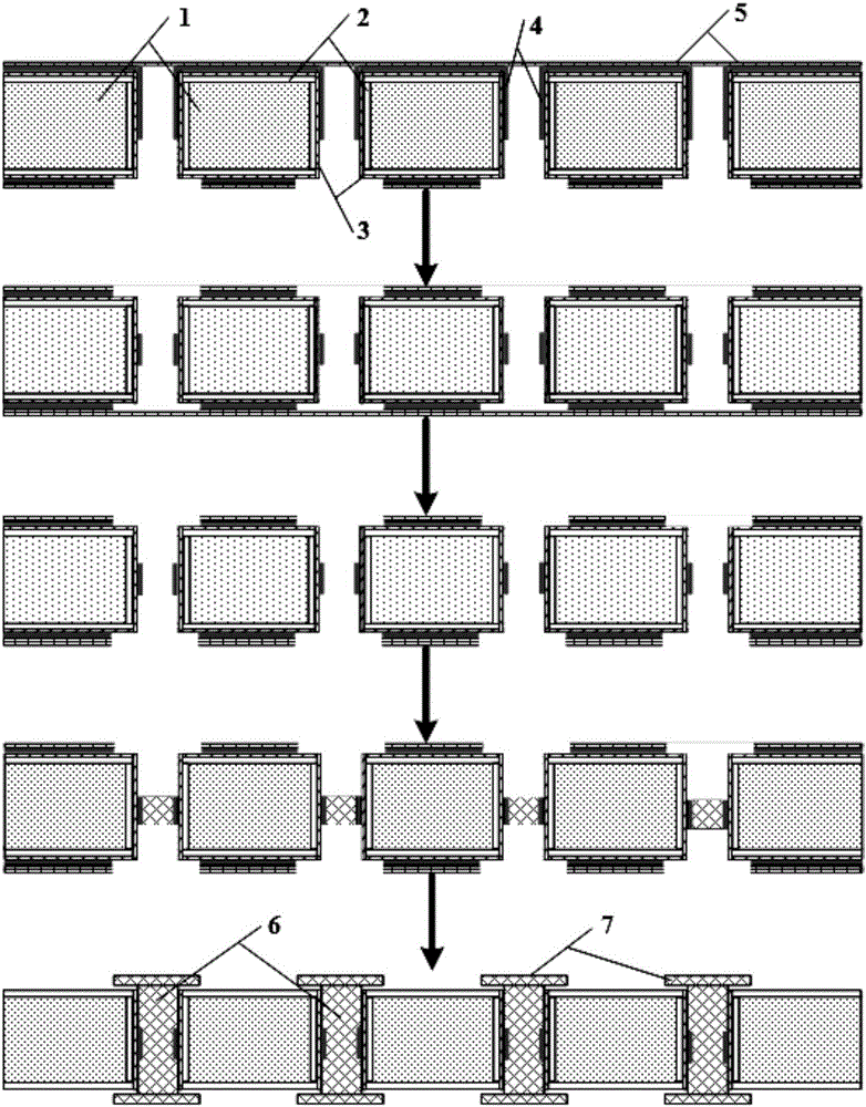
[0046] This embodiment provides a method for efficiently electroplating and filling silicon-based TSVs. Three times of TSV patterning are used to remove the seed layer at both ends of the TSV sidewall. Pre-wetting treatment is performed before electroplating. Perform bidirectional simultaneous blind via filling.

[0047] Described method specifically comprises the steps:

[0048] 1) Spin-coat positive resist with a thickness of 16 μm on the silicon wafer, bake the glue in a programmable oven, and perform photolithography and development on the baked wafer;

[0049] 2) using deep ion etching technology to etch TSVs on the wafer processed in step 1);

[0050] 3) high temperature oxidation is used to oxidize the surface of the wafer treated in step 2), and the oxidized thickness is 0.2 μm;

[0051] 4) on the wafer surface processed in step 3), carry out two-way sputtering Ti / Cu layer;

[0052] 5) paste dry film photoresist on both sides of the wafer after step 4), and then per...

Embodiment 2

[0064] This embodiment provides a method for efficiently electroplating and filling silicon-based TSVs. The previous steps are the same as in Embodiment 1, except that negative resist is selected as the coating, TSVs are etched by laser, and insulating films are deposited by chemical deposition techniques. The seed layer at the port portion of the side wall of the TSV is etched in a sealed pressure manner.

[0065] Described method specifically comprises the steps:

[0066] 1) Spin-coat the silicon wafer with a 10 μm negative glue, bake the glue in a programmable oven, and perform photolithography and development on the baked wafer;

[0067] 2) using laser technology to etch TSVs on the wafer processed in step 1);

[0068] 3) Depositing an insulating film on the surface of the wafer treated in step 2) by using chemical deposition technology, the thickness of the deposited insulating film is 0.21 μm;

[0069] 4) on the wafer surface processed in step 3), carry out two-way spu...


PUM

PropertyMeasurementUnit
Thicknessaaaaaaaaaa
Thicknessaaaaaaaaaa
Thicknessaaaaaaaaaa

Abstract

The invention discloses a method for efficiently electroplating and filling silicon-based TSV. The method specifically comprises the steps of etching and preparing the TSV on a wafer; preparing an insulating layer on the wafer for etching the TSV; preparing a seed layer on the wafer containing the insulating layer; enabling dry films to the adhered to the two surfaces of the wafer, and performing single-surface photoetching and developing; removing the seed layer from the TSV side wall port position; enabling the dry film to be adhered to the patterned surface and developing the other surface; removing the seed layer from the other port position again; then performing photoetching and developing again; next, performing bisynchronous electroplate copper filling to enable TSV-Cu and TSV-pad to be integrally molded without a separating interface; and removing the dry films, the photoresist and the seed layers. According to the method, the TSV through hole electroplating filling process is converted into two blind-hole-like electroplating filling processes, so that the TSV structure can be firmly combined; the process is more flexible and convenient; the high-aspect-ratio TSV through hole electroplating filling difficulty is greatly lowered; and meanwhile, the electroplating efficiency is effectively improved, and the low-cost and efficient TSV preparation can be realized.

Description

technical field [0001] The present invention relates to the field of microelectronic packaging, in particular, to a high-efficiency filling method based on through-holes, that is, a method for filling TSVs by bidirectional synchronous electroplating by dividing the middle of the through-holes into two blind holes. This method is suitable for low-cost silicon-based TSVs. Efficient fill preparation. Background technique [0002] With the rapid development of the semiconductor industry, the requirements for miniaturization and multi-functional integration of microsystems are increasingly urgent, with the advantages of high-speed interconnection, high-density integration, miniaturization, and homogeneous and heterogeneous functional integration. Packaging (3D-TSV) has gradually become one of the most popular researches in semiconductor packaging technology. Although 3D-TSV packaging technology has many advantages, there are still some unfavorable factors restricting the develop...

Claims


Application Information

Patent Timeline
IPC IPC(8): H01L21/768
CPCH01L21/76879H01L21/76898
Inventor 孙云娜王艳王博牛迪罗江波丁桂甫
Owner SHANGHAI JIAO TONG UNIV
Why Eureka
Try Eureka