Crystalline silicon preparation method and crystalline silicon

A technology of crystalline silicon and polycrystalline silicon, which is applied in the preparation of crystalline silicon and in the field of crystalline silicon, can solve the problems of low resistivity areas, low yield of crystalline silicon, non-concentrated resistivity distribution, etc.

Inactive Publication Date: 2016-07-13
JIANGXI SAI WEI LDK SOLAR HI TECH CO LTD
View PDF9 Cites 19 Cited by
  • Summary
  • Abstract
  • Description
  • Claims
  • Application Information

AI Technical Summary

Problems solved by technology

[0007] In view of this, the present invention provides a method for preparing crystalline silicon, which is used to solve the problem that the crystalline silicon prepared in the prior art has many areas with low resistivity, the distribution of resistivity is not concentrated, and the yield of crystalline silicon is low. question

Method used


Image

  • Crystalline silicon preparation method and crystalline silicon
  • Crystalline silicon preparation method and crystalline silicon
  • Crystalline silicon preparation method and crystalline silicon

Examples


Embodiment 1

[0075] A method for preparing gallium-doped monocrystalline silicon, comprising the following steps:

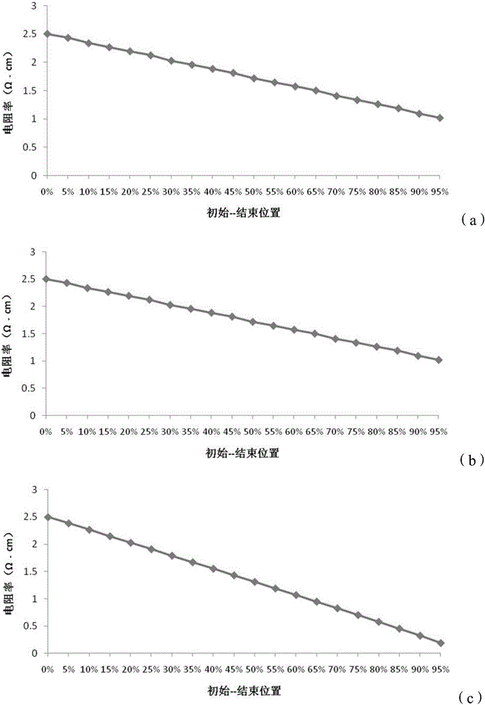
[0076] 1. Feeding: mix 120kg of polysilicon material and 4.02g of metal gallium (in each cubic centimeter of silicon material, the atomic volume concentration of gallium is 6.9E+17atoms / cm 3 ) into the quartz crucible of the single crystal furnace, the model of the crucible is a 24-inch quartz crucible, so that the target resistivity of the Czochralski silicon single crystal head is 2.5Ω cm; the single crystal furnace is also provided with a continuous A feeding device, putting molten second polysilicon material into the continuous feeding device;

[0077] 2. Under the protection of argon or nitrogen, heat the temperature to 1425°C-1600°C to melt the polysilicon material and metal gallium in the quartz crucible, so that the gallium element is melted into the polysilicon solution to form a silicon melt;

[0078] 3. Place a single crystal seed crystal on the upper surface of t...

Embodiment 2

[0088] A preparation method of gallium-doped polycrystalline silicon ingot, comprising the following steps:

[0089] 1. Feeding: Before feeding, the quartz crucible of G5 type (840mm×840mm inner diameter) is coated with silicon nitride, the thickness of the silicon nitride coating is 50 μm, and the purity is greater than 99.99%; 300kg of polysilicon material and 10g of Metal gallium dopant is put into described quartz crucible (in the silicon material of every cubic centimeter, the atomic volume concentration of gallium is 6.68E+17atoms / cm 3 ), so that the target resistivity of the tail of the polysilicon ingot is 2.6 Ω cm; the ingot furnace of the ingot furnace is also provided with a continuous feeding device, and the second polysilicon polysilicon melting is put into the continuous feeding device material;

[0090] 2. Melting: Transfer the crucible filled with raw materials to the ingot casting furnace with a forklift, and vacuumize the ingot casting furnace body, inject a...

Embodiment 3

[0099] A preparation method of gallium-doped polycrystalline silicon ingot, comprising the following steps:

[0100] Wherein, step 1-3 is with embodiment 2;

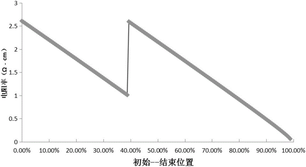
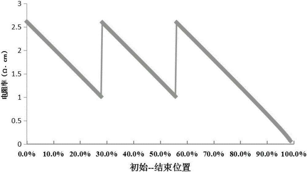
[0101] 4. Feeding for the first time: When the silicon melt crystallizes to 12cm, the weight of the crystallized silicon melt reaches 195kg, and the mass of the remaining silicon melt is 105Kg. At this time, the resistivity of the crystal reaches a critical The resistivity is 1.0Ω·cm, and 195Kg of polysilicon material is added to the crucible using a continuous feeding device, so that the resistivity of the crystal reaches the target resistivity of 2.6Ω·cm when the second crystal growth begins;

[0102] 5. Suspend the opening of the heat insulation cage, re-control the power of the heater, gradually increase the temperature in the furnace to 1500°C, and gradually melt the newly added polysilicon material in the crucible;

[0103] 6. The second crystal growth: when the newly added polysilicon material is completely melte...


PUM

PropertyMeasurementUnit
electrical resistivityaaaaaaaaaa
thicknessaaaaaaaaaa

Abstract

The invention provides a crystalline silicon preparation method.The crystalline silicon preparation method includes that polycrystalline silicon and a dopant are added into a crucible of a crystalline silicon ingot furnace or a single crystal furnace; in presence of protective gas, the polycrystalline silicon and the dopant are heated to melt completely to form silicon melts, crystalline silicon growth parameters are adjusted to enable the silicon melts to start to grow crystals, and in a crystal growing process, when resistivity of the crystals reaches clinical resistivity, new silicon melts formed by the polycrystalline silicon are replenished into residual silicon melts in the crucible to enable the resistivity of the crystals to be adjusted to target resistivity, and the new silicon melts continue growing crystals so as to obtain crystalline silicon with target yield after crystallization of the silicon melts in the crucible is completed.The crystalline silicon preparation method is capable of solving the problems of too many low-resistivity regions, scattered resistivity distribution and low crystalline silicon yield in the prior art.The invention further provides the crystalline silicon.

Description

technical field [0001] The invention relates to the technical field of solar cell materials, in particular to a method for preparing crystalline silicon and crystalline silicon. Background technique [0002] Among all kinds of solar cells in the photovoltaic industry, crystalline silicon (monocrystalline silicon, polycrystalline silicon) solar cells occupy an extremely important position, and currently occupy more than 75% of the photovoltaic market. Most of the silicon wafer materials for producing crystalline silicon solar cells are made of polycrystalline silicon ingots or processed from Czochralski silicon single crystals. [0003] For crystalline silicon solar cells, the photoelectric conversion efficiency is closely related to the resistivity of silicon wafers. Generally speaking, for the preparation of high-efficiency solar cells, the resistivity of crystalline silicon materials should be controlled in the range of 1-3Ω·cm, and the vertical distribution span of resis...

Claims


Application Information

Patent Timeline
Patent Type & Authority Applications(China)
IPC IPC(8): C30B15/02C30B15/20C30B28/06C30B29/06
CPCC30B15/02C30B15/20C30B28/06C30B29/06
Inventor 钟德京刘存健熊艳荣张涛邹军
Owner JIANGXI SAI WEI LDK SOLAR HI TECH CO LTD
Why Eureka
Try Eureka