GaN-based nanometer channel transistor with high electron mobility and manufacture method

A high electron mobility and nano-channel technology, applied in the field of microelectronic devices, can solve the problems of large leakage current, insufficient switching speed, and low transconductance, etc., and achieve small source-drain resistance, large saturation current, and gate control. The effect of good ability

Active Publication Date: 2016-07-13
XIDIAN UNIV
View PDF4 Cites 8 Cited by
  • Summary
  • Abstract
  • Description
  • Claims
  • Application Information

AI Technical Summary

Problems solved by technology

However, since the AlGaN/GaN heterojunction has a high concentration of two-dimensional electron gas 2DEG and has a high electron mobility, the leakage

Method used


Image

  • GaN-based nanometer channel transistor with high electron mobility and manufacture method
  • GaN-based nanometer channel transistor with high electron mobility and manufacture method
  • GaN-based nanometer channel transistor with high electron mobility and manufacture method

Examples


Embodiment 1

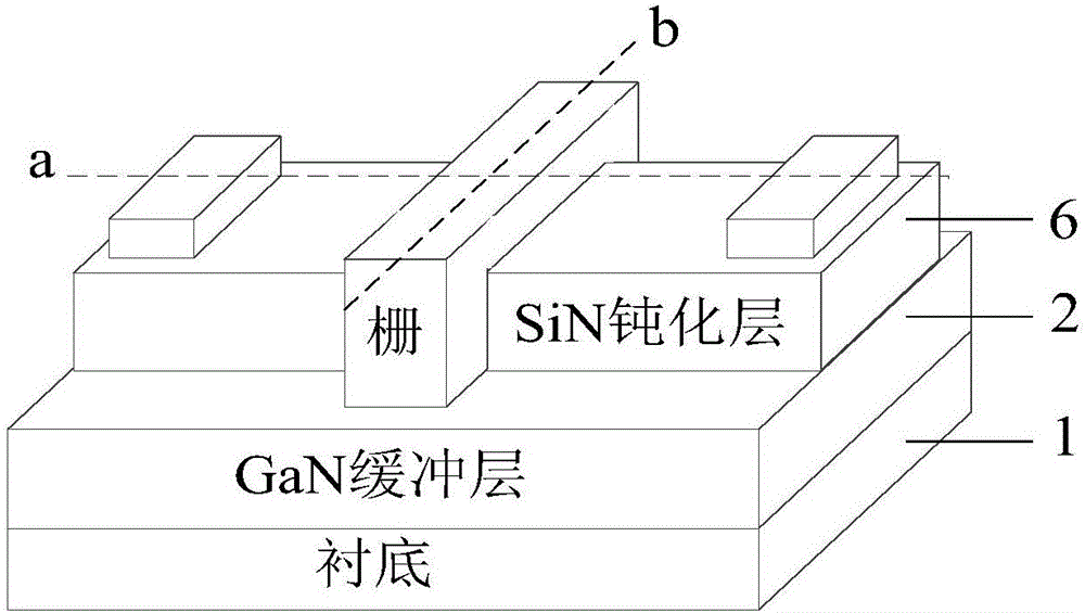
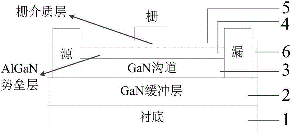
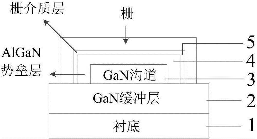
[0029] Embodiment 1: The production substrate is SiC, the thickness of the GaN buffer layer is 1 μm, the thickness of the GaN channel layer is 50 nm, the thickness of the AlGaN barrier layer is 15 nm, the Al composition is 30%, the thickness of the gate dielectric layer is 5 nm, and the passivation layer A high electron mobility device with a thickness of 50nm.

[0030] Step 1: A GaN buffer layer with a thickness of 1 μm is grown on the SiC substrate by metal-organic compound chemical vapor deposition MOCVD, and the process conditions are as follows:

[0031] The reaction gas is trimethylgallium and ammonia, the growth temperature is 800°C, and the pressure is 1.5×10 4 Pa.

[0032] Step 2: On the GaN buffer layer, a 50nm-thick GaN channel layer is grown on the GaN buffer layer by MOCVD, and the process conditions are as follows:

[0033] The reaction gas is trimethylgallium and ammonia, the growth temperature is 850°C, and the pressure is 1.5×10 4 Pa.

[0034] The growth r...

Embodiment 2

[0050] Embodiment 2: The production substrate is sapphire, the thickness of the GaN buffer layer is 1.2 μm, the thickness of the GaN channel layer is 70 nm, the thickness of the AlGaN barrier layer is 20 nm, the Al composition is 27%, the thickness of the gate dielectric layer is 7 nm, and the passivation Layer thickness is 75nm for high electron mobility devices.

[0051] Step 1: A GaN buffer layer with a thickness of 1.2 μm is grown on the sapphire substrate by metal-organic chemical vapor deposition MOCVD. The process conditions are: the reaction gas is trimethylgallium and ammonia, and the growth temperature is 800 ° C. The pressure is 1.5×10 4 Pa.

[0052] Step 2: On the GaN buffer layer, a 70nm-thick GaN channel layer is grown on the GaN buffer layer by MOCVD. The growth conditions are: the reaction gas is trimethylgallium and ammonia, and the growth temperature is 850°C The pressure is 1.5×10 4 Pa.

[0053] The growth results of the above steps 1 and 2 are as follow...

Embodiment 3

[0065] Embodiment 3: The production substrate is GaN, the thickness of the GaN buffer layer is 2 μm, the thickness of the GaN channel layer is 60 nm, the thickness of the AlGaN barrier layer is 20 nm, the Al composition is 22%, the thickness of the gate dielectric layer is 10 nm, and the passivation layer A high electron mobility device with a thickness of 100nm.

[0066] Step a: making a GaN buffer layer on the GaN substrate.

[0067] A layer of GaN buffer layer was grown on the GaN substrate by metal-organic compound chemical vapor deposition MOCVD. The growth process conditions were: the reaction gas was trimethylgallium and ammonia gas, the growth temperature was 800°C, and the pressure was 1.5×10 4 Pa, the thickness of the grown GaN buffer layer is 2 μm.

[0068] Step b: growing a GaN channel layer on the GaN buffer layer.

[0069] The GaN channel layer is grown on the GaN buffer layer by metal-organic compound chemical vapor deposition MOCVD. The growth process conditi...


PUM

PropertyMeasurementUnit
Thicknessaaaaaaaaaa
Thicknessaaaaaaaaaa
Widthaaaaaaaaaa

Abstract

The invention discloses a GaN-based nanometer channel transistor with high electron mobility and mainly aims at solving the problems that in the prior art, the short channel effect is serious, the grid control ability is poor, and the leak current and transconductance are low.The transistor comprises a substrate (1), a GaN buffer layer (2), a GaN channel (3), AlGaN barrier layers (4), a grid dielectric layer (5), a passivation layer (6), a source electrode, grid electrodes and a drain electrode from bottom to top.The AlGaN barrier layers are additionally arranged on the two sides of the GaN nanometer channel, the GaN nanometer channel is wrapped by the AlGaN barrier layers, and AlGaN/GaN heterojunctions are formed on the top and the two sides of the GaN nanometer channel; the grid electrodes are located on the two sides and the top of each AlGaN/GaN heterojunction.The transistor has the advantages of being good in grid control ability, large in saturation current and small in leak resistance, and can be used as a small-size high-speed high-frequency device.

Description

technical field [0001] The invention belongs to the technical field of microelectronic devices, in particular to a GaN-based nano-channel high electron mobility transistor HEMT, which can be used for high-frequency and high-speed integrated circuits. Background technique [0002] As a third-generation semiconductor material, GaN material is considered to be an excellent material for making microwave power devices and high-speed devices due to its advantages such as large band gap, high concentration of two-dimensional electron gas 2DEG and high electron saturation velocity. In particular, the AlGaN / GaN heterojunction high electron mobility transistor HEMT has a wide range of application values ​​in military and commercial applications. [0003] With the shrinking of the transistor size, the gate length is getting shorter and shorter, the short channel effect of the traditional high electron mobility transistor HEMT is becoming more and more obvious, which is manifested by th...

Claims


Application Information

Patent Timeline
IPC IPC(8): H01L21/335H01L29/20H01L29/778B82Y30/00
CPCB82Y30/00H01L29/2003H01L29/66431H01L29/7783
Inventor 张金风安阳黄旭张进成郝跃
Owner XIDIAN UNIV
Why Eureka
Try Eureka