

Organic optoelectronic material, preparation method thereof and organic light emitting diode containing organic material
A technology of organic optoelectronic materials and raw materials, applied in the direction of luminescent materials, electrical solid devices, electrical components, etc., can solve different problems and achieve the effects of avoiding close accumulation, high thermal stability, and high glass transition temperature
- Summary
- Abstract
- Description
- Claims
- Application Information
AI Technical Summary
Problems solved by technology
Method used
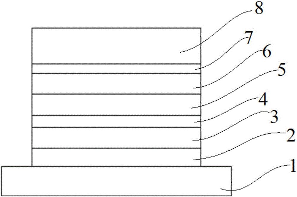
Image


Examples
Embodiment
[0102] The present application is further described below through specific examples. However, these examples are merely exemplary and do not constitute any limitation to the protection scope of the present application.
[0103] In the following examples and comparative examples, the reagents, materials and instruments used are conventional reagents, conventional materials and conventional instruments unless otherwise specified, and are commercially available, and the reagents involved can also be obtained through conventional Synthetic method obtained synthetically.
Embodiment 1
[0104] Embodiment 1. Preparation of organic optoelectronic materials
Embodiment 1
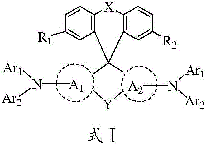
[0105] Example 1 Preparation of aforementioned compound 1
[0106] (1) Preparation of compound 1-a:
[0107]At -78°C and under the protection of nitrogen, 24.5g of 2-bromobiphenyl (105.0mmol) was dispersed in 500g of anhydrous tetrahydrofuran, and then 46mL of n-hexyl containing n-butyl lithium at a concentration of 2.5mol / L was added dropwise. Alkanes solution, after the dropwise addition, keep the reaction for 2.0 hours, and then at -60°C, add dropwise 300g of anhydrous tetrahydrofuran solution containing 29.2g of 2,7-tert-butylfluorenone (100mmol), and keep it for 2.0 hours after the dropwise reaction , then the reaction system was slowly warmed up to room temperature, and then poured into the system into 200g of dilute hydrochloric acid with a concentration of 2% by mass, stirred and reacted for 30min, then added 300g of ethyl acetate, the system was layered, washed with water, and finally the The organic phase was desolvated under reduced pressure until there was no fr...
PUM
| Property | Measurement | Unit |
|---|---|---|
| Thickness | aaaaa | aaaaa |
| Thickness | aaaaa | aaaaa |
Abstract
Description
Claims
Application Information