Double split trench gate charge storage type insulated gate bipolar transistor (IGBT) and manufacturing method thereof

A charge storage and charge storage layer technology, applied in semiconductor/solid-state device manufacturing, circuits, electrical components, etc., can solve problems such as reducing the switching speed of the device, increasing the switching loss of the device, and deteriorating the short-circuit safe working area of ​​the device.

Active Publication Date: 2016-07-20
UNIV OF ELECTRONIC SCI & TECH OF CHINA
View PDF6 Cites 6 Cited by
  • Summary
  • Abstract
  • Description
  • Claims
  • Application Information

AI Technical Summary

Problems solved by technology

However, for the CSTBT device structure, due to the existence of a higher doping concentration and a certain thickness of the N-type charge storage layer, the breakdown voltage of the device is significantly reduced. In order to effectively shield the adverse effects of the N-type charge storage layer to obtain a certain device withstand voltage , it is necessary to adopt: 1) deep trench gate depth, so that the depth of the trench gate is greater than the junction depth of the N-type charge storage layer, but the deep trench gate depth not only increases the gate-emitter capacitance, but also increases Therefore, the switching speed of the device is reduced, the switching loss of

Method used


Image

  • Double split trench gate charge storage type insulated gate bipolar transistor (IGBT) and manufacturing method thereof
  • Double split trench gate charge storage type insulated gate bipolar transistor (IGBT) and manufacturing method thereof
  • Double split trench gate charge storage type insulated gate bipolar transistor (IGBT) and manufacturing method thereof

Examples


Embodiment 1

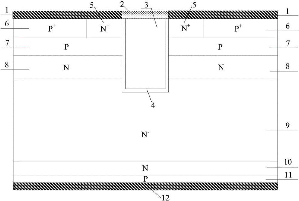
[0049] In this example, a double-split trench gate charge storage type IGBT, its cell structure is as follows figure 2As shown, it includes: the back collector metal 12, the P-type collector region 11 located on the back collector metal 12 and connected to it, the N-type field stop layer 10 located on the P-type collector region 11 and connected to it, The N-drift region 9 located on the N-type field stop layer 10 and connected to it; the compound double-split trench structure located in the middle of the upper part of the N-drift region 9 and connected to it; located on both sides of the upper part of the N-drift region 9 and connected to it The N-type charge storage layer 8, the sidewall of the N-type charge storage layer 8 is connected to the sidewall of the composite double split trench structure, the p-type base regions 71 and 72 located on the upper part of the N-type charge storage layer 8 and connected to it , the sidewalls of the p-type base regions 71 and 72 are con...

Embodiment 2

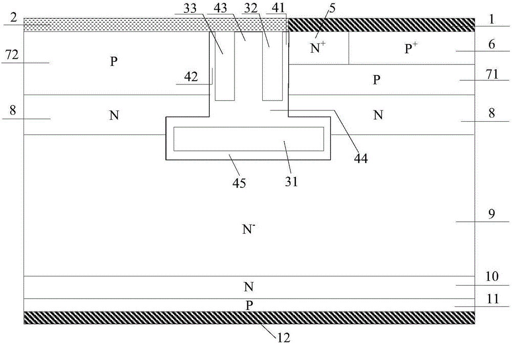
[0051] A double-split trench gate charge storage-IGBT in this example, its cell structure is as follows image 3 As shown, different from Embodiment 1, the lower part of the side split electrode 33 directly extends to the upper surface of the bottom split electrode 31, so that the side split electrode 33 and the bottom split electrode 31 are directly connected to further reduce the gate capacitance of the device.

Embodiment 3

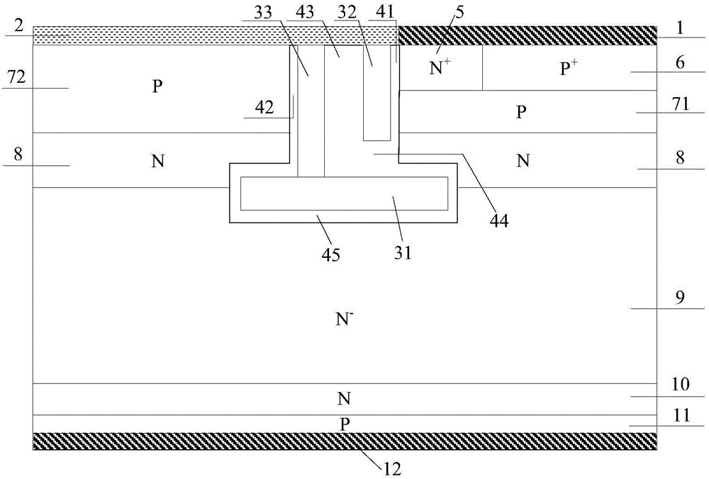
[0053] In this example, a double-split trench gate charge storage type IGBT, its cell structure is as follows Figure 4 As shown, different from Example 1, there is also a layer of N+ layer 13 in the partial region between the lower layer structure of the trench structure and the p-type base region 71, and the concentration of the N+ layer 13 is greater than that of the N-type charge concentration of the storage layer 8 and its sidewalls are connected to the composite trench structure, the formed N+ layer 13 further reduces the resistance of the area between the underlying structure of the composite trench structure and the p-type base region 71, and further improves the The carrier injection enhancement effect at the emitter end can achieve a better compromise between the device's forward voltage drop and switching loss.


PUM

PropertyMeasurementUnit
Thicknessaaaaaaaaaa
Thicknessaaaaaaaaaa

Abstract

The present invention belongs to the power semiconductor device technology field, in particular relates to a trench gate charge storage type IGBT. According to the present invention, by introducing a double split electrode equipotential with an emitter and a dielectric layer between the double split electrode and a gate electrode at the bottom and the side surface of the gate electrode in a device trench, and on the condition of not influencing the threshold voltage and the conduction of the IGBT, the grid capacitance is reduced, thereby improving the switching speed of the device, and reducing the switching loss of the device. Meanwhile, a wide bottom split electrode and a floating P-type base region further enable the carrier concentration distribution of a whole N-type drift region to be improved, and enable a short circuit safe operating area, a breakdown characteristic, the performance and the reliability of the device to be improved. The manufacturing method of the double split trench gate charge storage type IGBT provided by the present invention does not need the additional process steps, and is compatible with a conventional trench gate charge storage type insulated gate bipolar transistor manufacturing method.

Description

technical field [0001] The invention belongs to the technical field of power semiconductor devices, and relates to an insulated gate bipolar transistor (IGBT), in particular to a trench gate charge storage type insulated gate bipolar transistor (CSTBT). Background technique [0002] Insulated Gate Bipolar Transistor (IGBT) is a new type of power electronic device combining MOS field effect and bipolar transistor. It not only has the advantages of easy driving and simple control of MOSFET, but also has the advantages of low conduction voltage of power transistor, large on-state current and small loss. It has become one of the core electronic components in modern power electronic circuits and is widely used in Various fields of the national economy such as communications, energy, transportation, industry, medicine, household appliances and aerospace. The application of IGBT plays an extremely important role in improving the performance of power electronic systems. [0003] S...

Claims


Application Information

Patent Timeline
IPC IPC(8): H01L29/739H01L21/331
CPCH01L29/66348H01L29/7397
Inventor 张金平底聪田丰境刘竞秀李泽宏任敏张波
Owner UNIV OF ELECTRONIC SCI & TECH OF CHINA
Why Eureka
Try Eureka