Porous structure organic field effect transistor photosensitive memory and preparation method thereof

A porous structure and transistor technology, applied in semiconductor/solid-state device manufacturing, electric solid-state devices, semiconductor devices, etc., can solve the lack of research on the joint enhancement effect of photoresponse and storage characteristics, further explanation and systematic discussion, new material development costs Advanced problems, to achieve the effect of enhancing photoelectric conversion efficiency, increasing process complexity, improving storage performance and photosensitive performance

Inactive Publication Date: 2016-07-27
NANJING UNIV OF POSTS & TELECOMM
View PDF4 Cites 11 Cited by
  • Summary
  • Abstract
  • Description
  • Claims
  • Application Information

AI Technical Summary

Problems solved by technology

However, there are also disadvantages such as high cost of new material development, long cycle and complicated process, and relatively high equipment cost.
[0004] Judging from the overall research progress at home and abroad, OPTM still faces the following challenges: (1) The current research is still mainly focused on the storage phenomenon and storage behavior of OPTM, and there is a lack of research on the joint enhancement effect of photoresponse and storage characteristics ; (2) The operating voltage is too high (>100V), the light response speed is too slow (incident light>1s), the storage density is low (difficult to achieve multi-level storage), the light-dark current ratio is low (5 s); (3) The light-induced electrical storage mechanism needs to be further elucidated and systematically explored

Method used


Image

  • Porous structure organic field effect transistor photosensitive memory and preparation method thereof
  • Porous structure organic field effect transistor photosensitive memory and preparation method thereof
  • Porous structure organic field effect transistor photosensitive memory and preparation method thereof

Examples


Embodiment 1

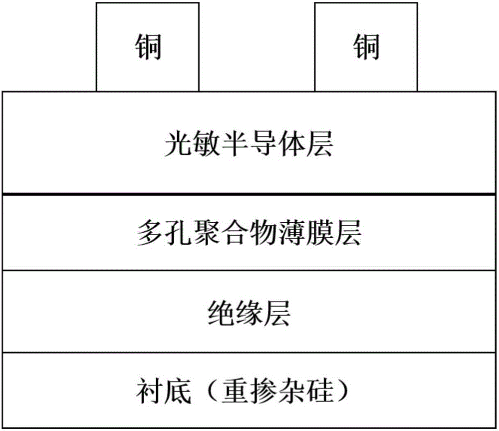
[0038] The present invention provides an organic field-effect transistor memory structure, and its structure diagram is as figure 1 Shown, including:

[0039] Substrate

[0040] A gate electrode formed on the substrate;

[0041] A gate insulating layer covering the gate electrode;

[0042] A polymer film layer with a porous structure formed on the gate insulating layer;

[0043] A porous organic photosensitive semiconductor layer formed on a porous polymer film layer; and

[0044] Porous source and drain electrodes formed on both sides of the channel region on the surface of the porous organic photosensitive semiconductor layer.

[0045] The substrate is a highly doped silicon wafer or glass wafer or plastic PET.

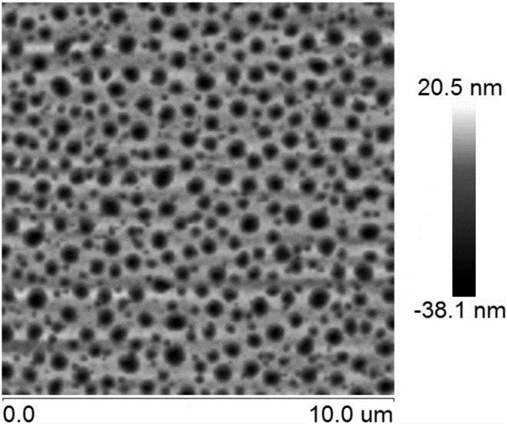
[0046] In the technical solution of this embodiment, heavily doped silicon is used as the substrate and gate electrode; a layer of 50-300nm silicon dioxide is used as the gate insulating layer; the polymer film layer with a porous structure is made of polymer polyethylene with a...

Embodiment 2

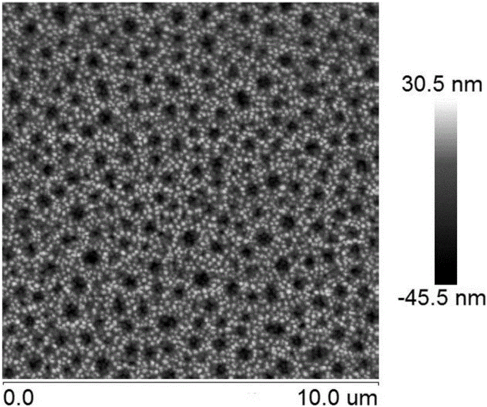
[0061] In the technical scheme of this embodiment, heavily doped silicon is used as the substrate and gate electrode; a layer of 50nm silicon dioxide is used as the gate insulating layer; the polymer film layer with porous structure is made of polymer polymethyl with porous structure. It is made of methyl acrylate (PMMA) with a thickness of 70nm; a 30nm thick pentacene layer is vapor-deposited on the gate insulating layer to serve as an organic photosensitive semiconductor layer; and then metal copper is vapor-deposited on both sides of the conductive channel as source and drain electrodes.

[0062] In the actual preparation, the laboratory room temperature is kept at about 25°C, and the indoor humidity is kept below 50%.

[0063] The specific preparation steps of the memory in this embodiment are as follows:

[0064] (1) Prepare PMMA solution, the concentration of the solution is 5mg / ml, and the solvent is tetrahydrofuran (THF) without additional water removal treatment and let stan...

Embodiment 3

[0070] In the technical solution of this embodiment, heavily doped silicon is used as the substrate and gate electrode; a layer of 50nm silicon dioxide is used as the gate insulating layer; the polymer film layer with a porous structure is made of a polymer polyvinyl group with a porous structure. It is composed of carbazole (PVK) with a thickness of 25nm; a layer of 50nm thick titanium bronze is vapor-deposited on the gate insulating layer to serve as an organic photosensitive semiconductor layer; and copper metal is vapor-deposited on both sides of the conductive channel as source and drain electrodes.

[0071] In the actual preparation, the laboratory room temperature is maintained at about 25°C, and the indoor humidity is maintained at 40%.

[0072] The specific preparation steps of the memory in this embodiment are as follows:

[0073] (1) Prepare polyvinyl carbazole (PVK) solution, the solution concentration is 5mg / ml, the solvent is chloroform (CHCl 3 ) Let stand for 24 hours ...


PUM


Abstract

The invention relates to a porous structure organic field effect transistor photosensitive memory and a preparation method thereof, and belongs to the field of semiconductor industry memory technologies and biofilm technologies. The memory comprises source and drain electrodes, an organic photosensitive semiconductor, a porous polymer film layer and a gate insulating layer which are arranged from top to bottom in sequence. The polymer film layer of a porous structure is arranged between the organic photosensitive semiconductor and the gate insulating layer. The source and drain electrodes and the organic photosensitive semiconductor are totally or partially of a porous structure which grows periodically. According to the invention, a spin-coating method is adopted to prepare the polymer film layer of the porous structure on a gate insulating layer substrate, and the polymer film layer is used as a porous template layer, the organic photosensitive semiconductor and the metal source and drain electrodes are induced to form the periodic porous growing features. The storage performance and the photosensitive performance of the device are improved by simple process means, the storage capacity, the switching speed and the light response capability are substantially improved, the preparation cost is lowered, and the popularization and the application are facilitated.

Description

Technical field [0001] The invention belongs to the field of memory technology and light detection technology in the semiconductor industry, and specifically relates to an organic field effect transistor photosensitive memory and a preparation method thereof. Background technique [0002] As the basic components in electronic circuits, organic field-effect transistors have the characteristics of wide material sources, softness and simple processing technology, and can be applied to large-area printing processes, which are very suitable for the development direction of the next generation of wearable electronics industry. At the same time, the structure of the organic field effect transistor determines that it has rich functional applications, such as light emitting, storage, sensing, switching, etc., so it has a wide range of application prospects in the field of information electronics. [0003] As a multifunctional integrated device, Organic Photosensitive Field Effect Transistor...

Claims


Application Information

Patent Timeline
Patent Type & Authority Applications(China)
IPC IPC(8): H01L51/10H01L27/28H01L27/30
CPCH10K39/30H10K19/10H10K10/84
Inventor 仪明东凌海峰解令海马洋杏包岩李焕群黄维
Owner NANJING UNIV OF POSTS & TELECOMM
Why Eureka
Try Eureka