
A high-dielectric gate dielectric material for flexible low-voltage driving organic thin film transistors and its preparation method and application

An organic thin film, low-voltage driven technology, applied in the field of organic electronics, can solve the problems of reducing the carrier mobility of the device, high annealing temperature of the dielectric layer, and high turn-on voltage of the device, and achieves large switching ratio, high mobility, The effect of a small subthreshold slope

Active Publication Date: 2018-10-30
SOUTH CHINA NORMAL UNIVERSITY
View PDF6 Cites 0 Cited by
  • Summary
  • Abstract
  • Description
  • Claims
  • Application Information

AI Technical Summary

Problems solved by technology

However, there are still problems to be solved: (1) the working voltage is too high, generally above 5V, and the turn-on voltage of the device is too high, resulting in large energy loss; (2) the annealing temperature of the dielectric layer of the solution spin coating is too high , high energy consumption, and unclean annealing, resulting in excessive leakage current and a corresponding decrease in switching ratio; (3) The stability and withstand voltage breakdown of the device still need to be improved
High-K gate dielectric materials have been widely studied and applied in Si-based MOSFETs. Using high-K materials to reduce the operating voltage of the device without reducing the carrier mobility of the device has become a new trend in domestic and foreign academic circles. However, the research on high-K materials in organic thin film transistors is still very limited. How to find a suitable high-K material to match with organic materials is also an important challenge for researchers.

Method used


Image

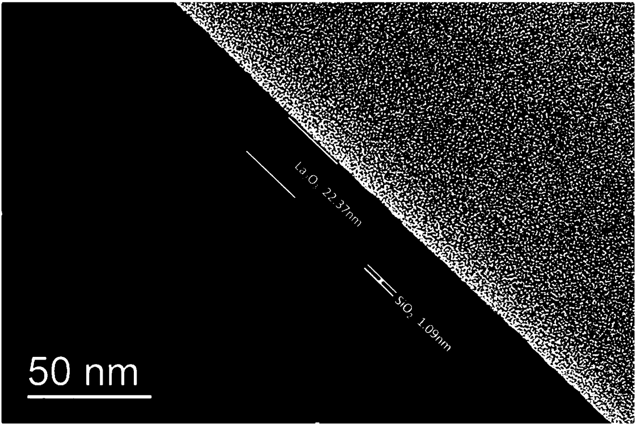
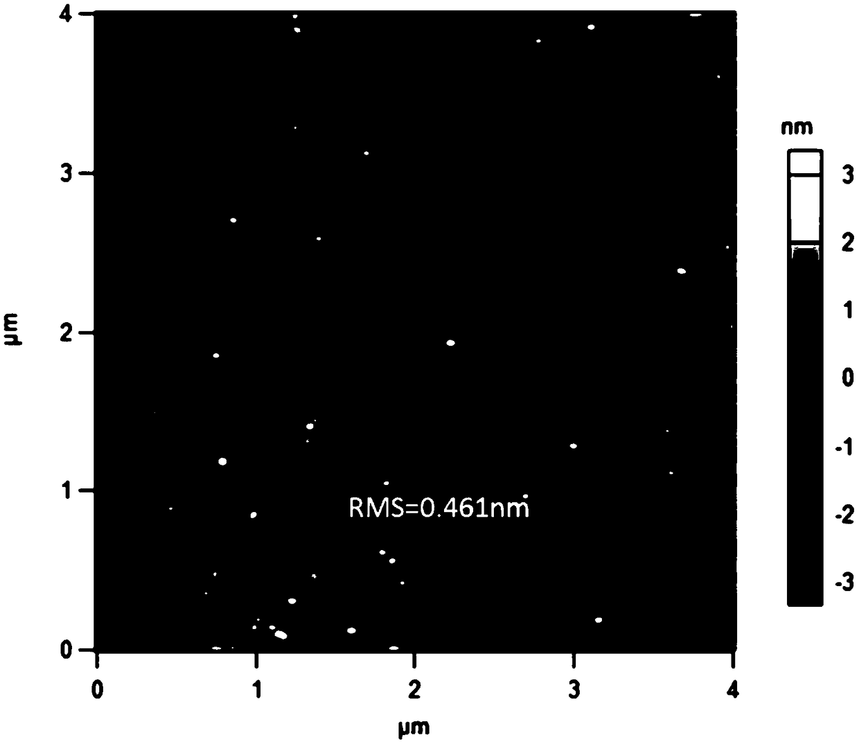
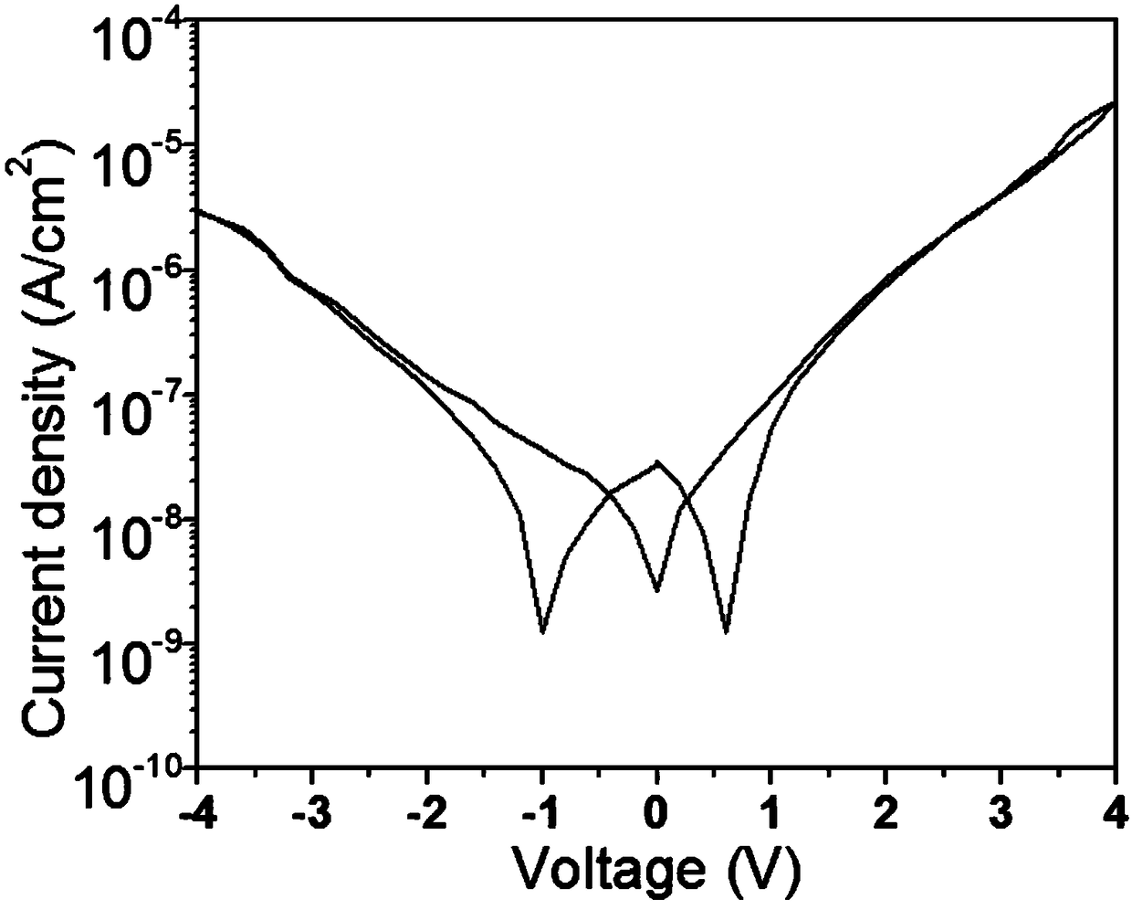
  • A high-dielectric gate dielectric material for flexible low-voltage driving organic thin film transistors and its preparation method and application
  • A high-dielectric gate dielectric material for flexible low-voltage driving organic thin film transistors and its preparation method and application
  • A high-dielectric gate dielectric material for flexible low-voltage driving organic thin film transistors and its preparation method and application

Examples


Embodiment 1

[0048] This embodiment provides a method for preparing a flexible low-voltage drive organic thin film transistor, including the following steps:

[0049] 1) Depositing the bottom gate electrode on the cleaned substrate: specifically including the following steps:

[0050] 1a) Select a flexible PET substrate and cut it into a square block of 1.5cm×1.5cm;

[0051] 1b) The substrate was ultrasonically cleaned with acetone, isopropanol, deionized water, and ethanol in sequence, then dried in an oven, and then subjected to UV / O 3 After activation, save it for later use;

[0052] 1c) A 40 nm thick Au bottom-gate electrode was deposited on a cleaned PET substrate by thermal evaporation; the deposition was carried out under high vacuum with an air pressure of 6 × 10 -4 Pa, the deposition rate is 0.02nm / s;

[0053] 2) Preparation of lanthanum oxide precursor solution: use lanthanum acetylacetonate as the solute, N,N-dimethylformamide (DMF) as the solvent, prepare a solution with a m...

Embodiment 2

[0061] This embodiment provides a method for preparing a flexible low-voltage drive organic thin film transistor, including the following steps:

[0062] 1) Depositing the bottom gate electrode on the cleaned substrate: specifically including the following steps:

[0063] 1a) Select a flexible PET substrate and cut it into a square block of 1.5cm×1.5cm;

[0064] 1b) The substrate was ultrasonically cleaned with acetone, isopropanol, deionized water, and ethanol in sequence, then dried in an oven, and then subjected to UV / O 3 After activation, save it for later use;

[0065] 1c) A 40 nm thick Au bottom-gate electrode was deposited on a cleaned PET substrate by thermal evaporation; the deposition was carried out under high vacuum with an air pressure of 6 × 10 -4 Pa, the deposition rate is 0.01nm / s;

[0066] 2) Preparation of lanthanum oxide precursor solution: use lanthanum acetylacetonate as the solute, N,N-dimethylformamide (DMF) as the solvent, prepare a solution with a m...

Embodiment 3

[0074] This embodiment provides a method for preparing a flexible low-voltage drive organic thin film transistor, including the following steps:

[0075] 1) Depositing the bottom gate electrode on the cleaned substrate: specifically including the following steps:

[0076] 1a) Select a flexible PET substrate and cut it into a square block of 1.5cm×1.5cm;

[0077] 1b) The substrate was ultrasonically cleaned with acetone, isopropanol, deionized water, and ethanol in sequence, then dried in an oven, and then subjected to UV / O 3 After activation, save it for later use;

[0078] 1c) A 40 nm thick Au bottom-gate electrode was deposited on a cleaned PET substrate by thermal evaporation; the deposition was carried out under high vacuum with an air pressure of 6 × 10 -4 Pa, the deposition rate is 0.03nm / s;

[0079] 2) Preparation of lanthanum oxide precursor solution: use lanthanum acetylacetonate as the solute, N,N-dimethylformamide (DMF) as the solvent, prepare a solution with a m...


PUM

PropertyMeasurementUnit
thicknessaaaaaaaaaa
thicknessaaaaaaaaaa
thicknessaaaaaaaaaa

Abstract

The invention relates to a high-dielectric gate dielectric material for flexible low-voltage driving organic thin film transistors and a preparation method thereof, comprising the following steps: 1) preparing a lanthanum oxide precursor solution; 2) preparing a lanthanum oxide dielectric layer film: combining step 1) After the obtained lanthanum oxide precursor solution is filtered, the lanthanum oxide precursor solution is spin-coated on the substrate to obtain a lanthanum oxide precursor film; 3) the samples obtained in step 2) are sequentially subjected to pre-annealing treatment, heat treatment and ozone activation treatment Finally, a lanthanum oxide dielectric layer is obtained, that is, a high dielectric gate dielectric material is obtained. The high-dielectric gate dielectric material lanthanum oxide dielectric layer of the present invention has a high dielectric constant and a wide energy band, which can effectively reduce the working voltage required by the device; and it is prepared by a solution method, and can form a dense Non-toxic thin film, simple process and low cost. The invention also provides a flexible low-voltage driving organic thin film transistor using the high-dielectric gate dielectric material as a dielectric layer and a preparation method thereof.

Description

technical field [0001] The invention belongs to the technical field of organic electronics, and in particular relates to a high-dielectric gate dielectric material for flexible low-voltage driving organic thin film transistors, a preparation method and application thereof. Background technique [0002] Organic electronic flexible devices have received extensive attention from academia and social industry in the past 20 years, and they are an important development direction of flexible electronic display devices in the future. Great progress has been made, such as organic field effect transistors, organic solar cells, biosensors, TFT arrays, organic light-emitting diodes, etc. At present, organic materials and devices have gradually moved from basic research to industrialization. In application production, they have the characteristics of simple manufacturing process, flexibility, variety and low cost; as the processing and annealing temperature of the device decreases, the r...

Claims


Application Information

Patent Timeline
Patent Type & Authority Patents(China)
IPC IPC(8): H01L51/05H01L51/40H01L21/02
CPCH01L21/02192H01L21/02282H01L21/02318H01L21/02337H10K10/472
Inventor 陆旭兵严龙森龚岩芬曾敏刘俊明
Owner SOUTH CHINA NORMAL UNIVERSITY
Learn More