Preparation methods of electromagnetic shielding film and electromagnetic shielding window

A technology of electromagnetic shielding film and electromagnetic shielding window, applied in the fields of magnetic field/electric field shielding, chemical instruments and methods, photoengraving process of pattern surface, etc. The effect of surface resistance and high light transmittance

Inactive Publication Date: 2016-10-26
SUZHOU UNIV +1
View PDF13 Cites 20 Cited by
  • Summary
  • Abstract
  • Description
  • Claims
  • Application Information

AI Technical Summary

Problems solved by technology

In the past, the metal grid structure was attached to the surface of the flexible substrate. Under this bending radius, the metal grid structure is easy to separate from the flexible substrate, which is difficult to meet the application requirements in the field of flexible electronics.

Method used


Image

  • Preparation methods of electromagnetic shielding film and electromagnetic shielding window
  • Preparation methods of electromagnetic shielding film and electromagnetic shielding window
  • Preparation methods of electromagnetic shielding film and electromagnetic shielding window

Examples


Embodiment 1

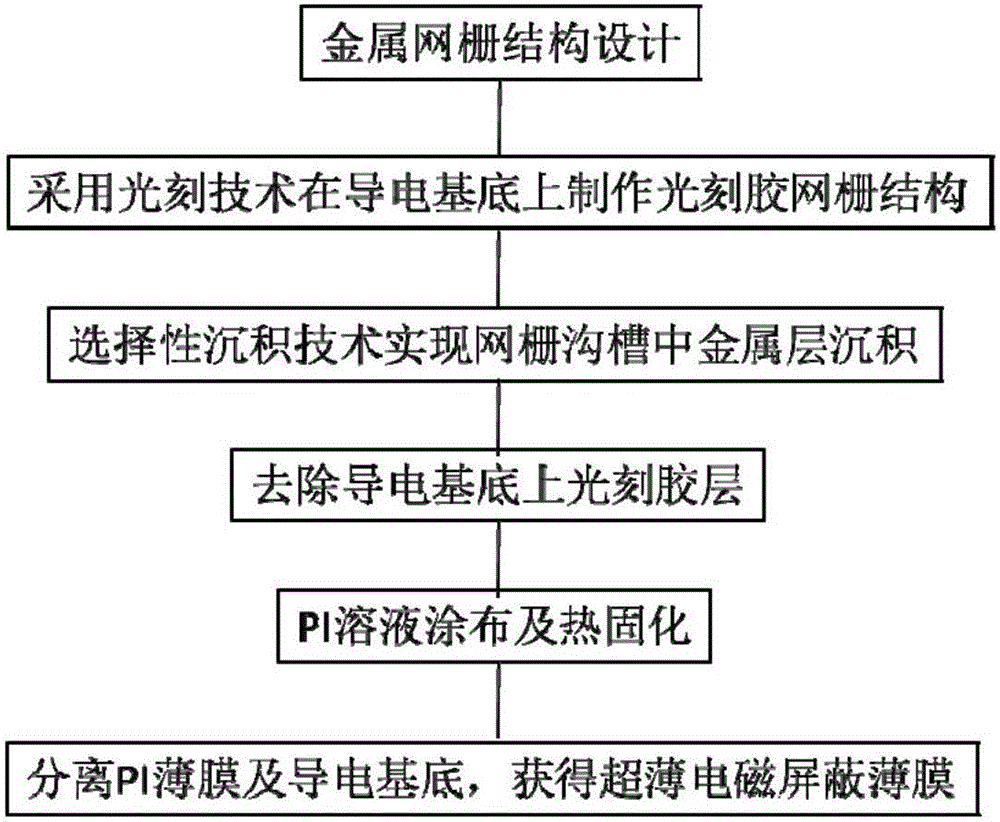
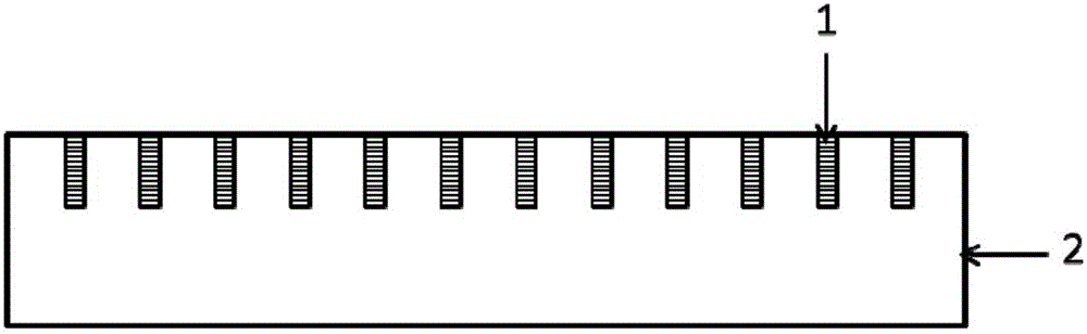
[0056] Embodiment 1: Ultra-thin metal grid electromagnetic shielding film. Production process such as figure 1 As shown, firstly, according to the requirement of shielding effectiveness, design the arrangement of the metal grid structure, which can be hexagonal, square, rectangular, parallelogram, triangular, etc. periodic arrangement, or arbitrary multi-deformation arrangement, etc., the grid structure Line width (300nm-10μm), grid spacing (1-500μm) and other parameters, and then patterned on the conductive substrate coated with photoresist by patterning (laser direct writing, ultraviolet exposure, electron beam exposure, etc.) technology grid structure. The patterned conductive substrate is placed on the cathode of the electrodeposition tank, and the metal material (nickel, copper, gold, aluminum, silver, etc.) to be deposited is placed on the anode. Using the selective depositability of electrodeposition, the metal on the anode is gradually deposited on the cathode by cati...

Embodiment 2

[0058] Embodiment 2, a metal grid type electromagnetic shielding film embedded in an ultraviolet curing glue. According to the manufacturing process of Embodiment 1, a metal grid structure is fabricated on a conductive substrate through a selective electrodeposition process. According to the design requirements, the line width (300nm-10μm) of the metal grid, the grid spacing (10-500μm), and the thickness of the metal deposition layer (300nm-10μm) are formed. Then, the UV-curable glue is coated on the deposited and deglued conductive substrate, and the PET film is covered thereon, and irradiated with a UV lamp. The UV-curable glue is cured after being irradiated with light, and adheres to the PET substrate3. After the PET and the conductive substrate are peeled off, the metal grid 4 is embedded in the ultraviolet curing adhesive 5 to form an electromagnetic shielding film, such as image 3 shown. The transmittance of the electromagnetic shielding film is determined by the ra...

Embodiment 3

[0060] Embodiment 3, embedded electromagnetic shielding film. According to the manufacturing process of Embodiment 1, a metal grid structure is fabricated on a conductive substrate through a selective electrodeposition process. According to the design requirements, the line width (300nm-10μm) of the metal grid, the grid spacing (10-500μm), and the thickness of the metal deposition layer (300nm-10μm) are formed. Then cover the COC film on the deposited and deglued conductive substrate, and apply a certain temperature (over the glass transition temperature of the COC film) and pressure. By hot embossing technology, the metal grid is embedded inside the COC film. After the COC film is separated from the conductive substrate, an electromagnetic shielding film embedded in the COC is obtained.


PUM

PropertyMeasurementUnit
diameteraaaaaaaaaa
radiusaaaaaaaaaa
thicknessaaaaaaaaaa

Abstract

The invention discloses a preparation method of an electromagnetic shielding film. The method comprises the steps of 1), coating photoresist on a conductive substrate, and forming a pattern structure on the conductive substrate through a lithography technology; 2), growing a metal layer in the pattern structure through a selective electro-deposition technology, thereby forming a metal pattern structure; and 3), embedding the metal pattern structure in a flexible base material through an embossing technology, thereby forming the electromagnetic shielding film. The invention also discloses a preparation method of an electromagnetic shielding window. The methods have the advantages of high transparency and high temperature resistance. According to the methods, demands of an optical window for high shielding performance, high imaging quality and high temperature resistance of the electromagnetic shielding film can be satisfied. The demand of flexible electronics for bending performance of the electromagnetic shielding film can be satisfied. The demand of surface mounting of a complex structure for ultrathin property of the shielding film can be satisfied.

Description

technical field [0001] The invention relates to a film manufacturing technology, in particular to a manufacturing method of an electromagnetic shielding film and an electromagnetic shielding window. Background technique [0002] With the rapid development of the modern electronic industry, electronic products and wireless communication equipment can be popularized, so that the application band of electronic waves continues to expand, while the intensity further increases, making the space electromagnetic environment increasingly complex. Electromagnetic radiation pollution has been paid more and more attention. Electromagnetic waves not only interfere with the normal operation of various electronic equipment, but also threaten the information security of communication equipment, and even endanger human health in severe cases. In order to prevent electromagnetic waves from leaking and causing electromagnetic hazards, electromagnetic shielding materials are currently used to s...

Claims


Application Information

Patent Timeline
Patent Type & Authority Applications(China)
IPC IPC(8): H05K9/00
CPCH05K9/0086B32B2307/212B32B2307/202B32B17/061B32B17/10G03F7/40G03F7/2053H05K9/0088G03F7/0002B32B17/10036B32B17/10165B32B17/10889B32B17/10981G03F7/405G03F7/422
Inventor 刘艳花陈林森王波沈悦周云周小红叶燕方宗豹
Owner SUZHOU UNIV
Why Eureka
Try Eureka