

An ultraviolet light-emitting diode with p-region structure
A technology for light-emitting diodes and structural electronics, which is applied in the fields of nanotechnology, electrical components, nanotechnology, etc. for materials and surface science, and can solve the problem of preparing ultraviolet light-emitting diodes without a p-type ZnMgNiO layer structure, and electrons overflowing into the active area. And the problems of low hole injection efficiency and efficiency decay, etc., to achieve high lateral carrier mobility, improve recombination efficiency, and reduce separation effects
- Summary
- Abstract
- Description
- Claims
- Application Information
AI Technical Summary
Problems solved by technology
Method used
Image

Examples
Embodiment Construction
[0021] The following will clearly and completely describe the technical solutions in the embodiments of the present invention with reference to the accompanying drawings in the embodiments of the present invention. Obviously, the described embodiments are only some, not all, embodiments of the present invention. Based on the embodiments of the present invention, all other embodiments obtained by persons of ordinary skill in the art without making creative efforts belong to the protection scope of the present invention.
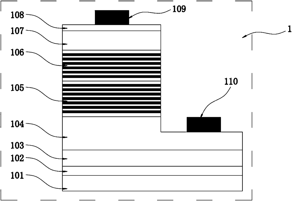
[0022] see Figure 1-2 , the present invention provides a technical solution:
[0023] An ultraviolet light-emitting diode with a p-region structure, comprising a tube body 1, which is sequentially provided with a sapphire substrate 101, an AlN nucleation layer 102, an undoped u-type AlGaN buffer layer 103, and an n-type AlGaN layer 104 from bottom to top 、Al x1 Ga 1-x1 N / Al x2 Ga 1-x2 N quantum well active region 105, p-type Zn y1 Mg 1-y1 O / Al x3 Ga ...
PUM
 Abstract
Description
Claims
Application Information