Method for preparing black silicon structure by Ag-Cu (silver-copper) bimetallic MACE (metal-assisted chemical etching) type

A bi-metal, black silicon technology, applied in chemical instruments and methods, final product manufacturing, sustainable manufacturing/processing, etc., can solve problems such as restricting the efficiency of black silicon cells and the inability of thin films to passivate the black silicon surface well. To achieve the effect of reducing the preparation cost, reducing the dosage, and improving the conversion efficiency

Active Publication Date: 2016-12-14
NANJING UNIV OF AERONAUTICS & ASTRONAUTICS
View PDF2 Cites 17 Cited by
  • Summary
  • Abstract
  • Description
  • Claims
  • Application Information

AI Technical Summary

Problems solved by technology

Current passivation process, PECVD deposited Si x N y The thin film cannot passivate the surface o

Method used


Image

  • Method for preparing black silicon structure by Ag-Cu (silver-copper) bimetallic MACE (metal-assisted chemical etching) type
  • Method for preparing black silicon structure by Ag-Cu (silver-copper) bimetallic MACE (metal-assisted chemical etching) type
  • Method for preparing black silicon structure by Ag-Cu (silver-copper) bimetallic MACE (metal-assisted chemical etching) type

Examples


preparation example Construction

[0028]In order to control the preparation cost of black silicon and improve the conversion efficiency of black silicon cells, an embodiment of the present invention provides a low-cost silver-copper bimetallic MACE method for preparing a polycrystalline black silicon structure, including:

[0029] Clean the surface of the silicon wafer;

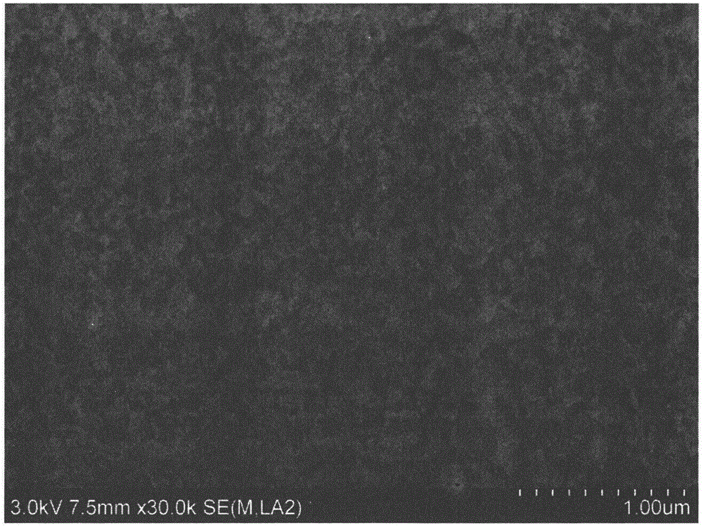
[0030] Using Cu(NO 3 ) 2 and AgNO 3 The MACE etching solution of bimetallic atoms catalyzes the corrosion of silicon wafers to prepare nanoporous structures;

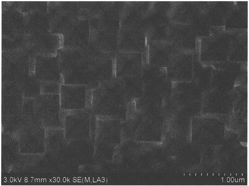
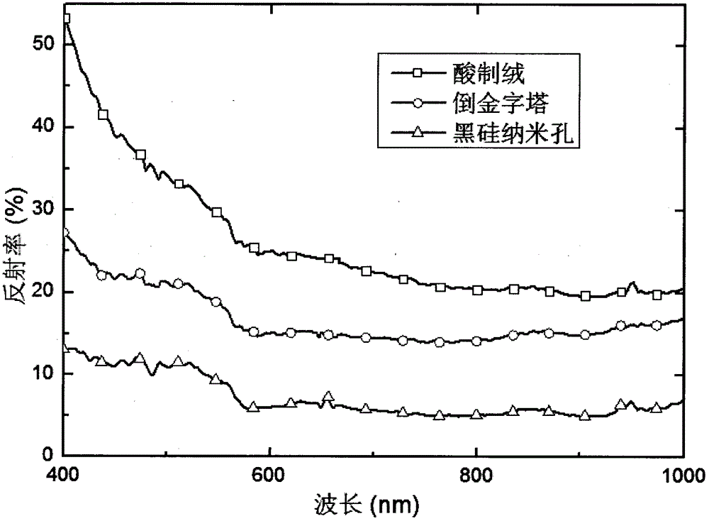
[0031] The prepared black silicon is cleaned with a nano-reconstruction solution to form an inverted pyramid anti-reflection structure on the surface of the silicon wafer.

[0032] The principle of the present invention: because the electronegativity of silicon is 1.90, when metal elements such as Ag (1.93), Cu (1.91) etc. with higher electronegativity than silicon are in contact with silicon and are in HF and H 2 o 2 When in the mixed solution of silicon, a galvanic cell will be ...

Embodiment 1

[0039] (1) First use acidic hydrogen peroxide containing sulfuric acid for acid oxidation cleaning, then use weak alkaline hydrogen peroxide containing amine for alkaline oxidation cleaning, then use dilute hydrofluoric acid solution for cleaning, and finally use hydrochloric acid Acidic hydrogen peroxide is used for acidic oxidation cleaning, rinsing with ultrapure water (DI water) in the middle of each cleaning, and finally drying with low boiling point organic solvents.

[0040] (2) Dip the cleaned silicon wafer into solution 1 for corrosion, 0.1mM AgNO 3 +24mM Cu(NO 3 ) 2 +5M HF+0.4MH 2 o 2 , controlling the molar ratio of silver and copper ions to be 1:240 to obtain nanopore and nanogroove structures, the reaction time is 180s, and the reaction temperature is room temperature;

[0041] (3) immerse the etched black silicon chip in the solution to clean, remove residual silver nanoparticles, H 2 o 2 : NH 4 OH=1:3, the reaction time is 180s;

[0042] (4) Immersing th...

Embodiment 2

[0046] (1) First use acidic hydrogen peroxide containing sulfuric acid for acid oxidation cleaning, then use weak alkaline hydrogen peroxide containing amine for alkaline oxidation cleaning, then use dilute hydrofluoric acid solution for cleaning, and finally use hydrochloric acid Acidic hydrogen peroxide is used for acidic oxidation cleaning, rinsing with ultrapure water (DI water) in the middle of each cleaning, and finally drying with low boiling point organic solvents.

[0047] (2) Dip the cleaned silicon wafer into solution 1 for corrosion, 0.1mM AgNO 3 +24mM Cu(NO 3 ) 2 +5M HF+0.4MH 2 o 2 , controlling the molar ratio of silver and copper ions to be 1:240 to obtain nanopore and nanogroove structures, the reaction time is 180s, and the reaction temperature is room temperature;

[0048] (3) immerse the etched black silicon chip in the solution to clean, remove residual silver nanoparticles, H 2 o 2 : NH 4 OH=1:3, the reaction time is 180s;

[0049] (4) Immersing th...


PUM

PropertyMeasurementUnit
Apertureaaaaaaaaaa
Hole depthaaaaaaaaaa
Apertureaaaaaaaaaa

Abstract

The invention relates to a method for preparing a black silicon structure with low cost, and belongs to the technical field of photoelectricity. The method comprises the following steps of (1) precleaning a solution; (2) putting the cleaned silicon chip into a mixing solution of H2O2 (hydrogen peroxide), HF (hydrogen fluoride), AgNO3 (silver nitrate), Cu(NO3)2 (copper dinitrate) and ultrapure water, and etching, so as to prepare a black silicon nanometer antireflection structure; (3) optimizing the black silicon structure by a nanometer reconstruction solution, so as to form a uniform inverted pyramid-shaped structure. The method has the advantages that the polycrystalline silicon is performed with chemical etching by an Ag-Cu bimetallic assisting type; compared with the existing Ag-assisted chemical etching type, the consumption amount of AgNO3 is decreased by more than several dozens of times; the technology is simple, the preparation cost of black silicon is reduced, and the batch preparation of large-area black silicon is reduced; the black silicon structure is optimized by the nanometer reconstruction solution, and the huge application potential is realized in the preparation of black silicon solar batteries with high conversion efficiency.

Description

technical field [0001] The invention relates to a low-cost method for preparing a black silicon structure, which belongs to the field of photoelectric technology. The invention adopts Ag and Cu dual metals to assist chemical etching on the surface of polysilicon. Compared with the existing Ag-assisted chemical etching, this invention enables AgNO 3 The consumption is reduced by more than dozens of times, and the process is simple, which reduces the cost of black silicon preparation, and can realize the batch preparation of large-area black silicon, and the method of optimizing the structure of black silicon with nano-reconstruction solution, in the case of high conversion efficiency There is great application potential in the preparation of black silicon solar cells. Background technique [0002] At present, the photovoltaic power generation of crystalline silicon (monocrystalline and polycrystalline) solar cells is the mainstream field of photovoltaic power generation, but...

Claims


Application Information

Patent Timeline
IPC IPC(8): H01L31/18H01L31/0236C30B33/10
CPCC30B33/10H01L31/0236H01L31/02363H01L31/18Y02E10/50Y02P70/50
Inventor 沈鸿烈郑超凡蒲天蒋晔吴兢
Owner NANJING UNIV OF AERONAUTICS & ASTRONAUTICS
Why Eureka
Try Eureka