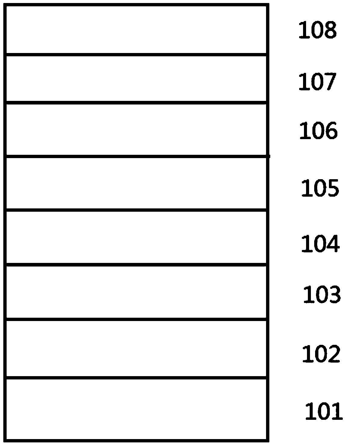
A method for preparing p-type algan/alingan electron blocking layer near-ultraviolet leds with doping concentration and al component stepwise change
A technology of electron blocking layer and doping concentration, applied in circuits, electrical components, semiconductor devices, etc., can solve the problem of output power only input power
- Summary
- Abstract
- Description
- Claims
- Application Information
AI Technical Summary
Problems solved by technology
Method used
Image
Examples
Embodiment 1
[0019] Using Aixtron’s close-coupled vertical reaction chamber MOCVD growth system, trimethylgallium (TMGa), triethylgallium, trimethylaluminum, trimethylindium and ammonia were used as Ga, Al, In and N source, silane (SiH 4 ) as an n-type dopant source, dimagnesocene (Cp 2 Mg) as a p-type dopant source, the patterned Al 2 o 3 The substrate 101 is heated to 1080-1100 degrees centigrade, and the pressure in the reaction chamber is 100 torr. 2 Under treatment for 5 minutes, then cool down to 530-550 degrees Celsius in the patterned Al 2 o 3 On the substrate 101, the pressure of the reaction chamber is 500 torr, the hydrogen (H2) atmosphere, the V / III molar ratio is 500-1300, and the low-temperature GaN nucleation layer 102 after three-dimensional growth of 20-30 nm is reacted at 1000-1500 ° C The chamber pressure is 200-300torr, in hydrogen (H 2 ) atmosphere, the V / III molar ratio is 1000-1300; grow a high-temperature non-doped GaN buffer layer 103 with a thickness of 2-4 ...
PUM
 Abstract
Description
Claims
Application Information
