Method of adopting plasma technology to treat silver nanowires and transferring through substrate to prepare organic photoelectronic device flexible electrode

A silver nanowire and plasma technology, which is applied in the manufacture of semiconductor devices, electric solid-state devices, and semiconductor/solid-state devices, etc., can solve the problems of excessive heat generation, high surface roughness of silver nanowire films, and burnt-out devices.

Inactive Publication Date: 2017-01-04
JILIN UNIV
View PDF5 Cites 5 Cited by
  • Summary
  • Abstract
  • Description
  • Claims
  • Application Information

AI Technical Summary

Problems solved by technology

At the junction where more silver nanowires intersect, the surface height will be higher than other positions, which will cause the surface roughness of the silver nanowire film to be too high, and the surface conductivity will be uneven
For OLED devices, because the overall thickness of the device is very small, only a few hundred nanometers, if the surface roughness of the electrode is too large, the electrode layer may penetrate the hole transport layer or even the light-emitting layer, causing the device to fail during the light-emitting process. point
If the surface conductivity is uneven, it will cause excessive local current, excessive heat, and burn out the device

Method used


Image

  • Method of adopting plasma technology to treat silver nanowires and transferring through substrate to prepare organic photoelectronic device flexible electrode
  • Method of adopting plasma technology to treat silver nanowires and transferring through substrate to prepare organic photoelectronic device flexible electrode
  • Method of adopting plasma technology to treat silver nanowires and transferring through substrate to prepare organic photoelectronic device flexible electrode

Examples


Embodiment 1

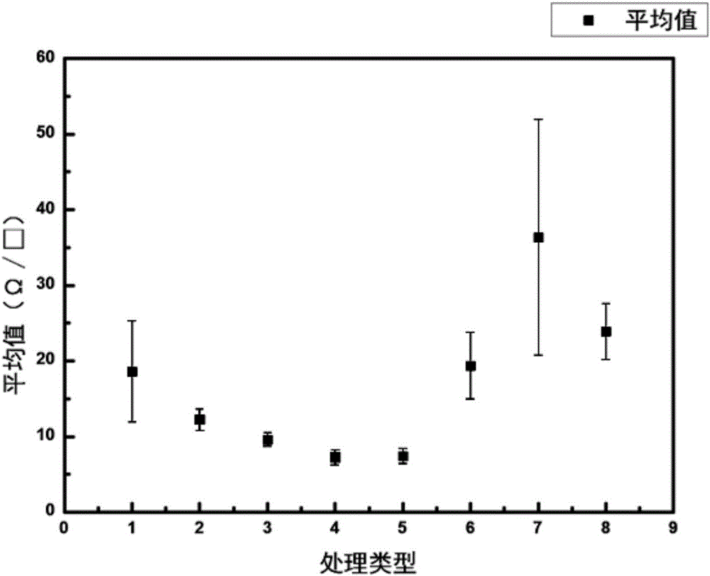
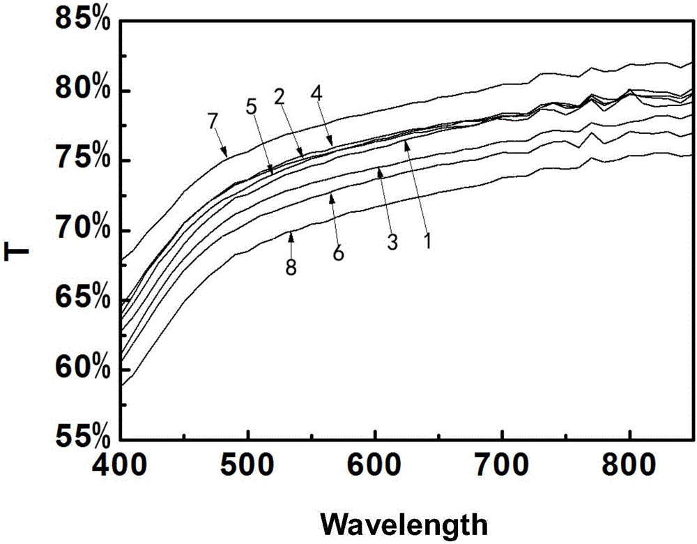
[0024] In order to verify the feasibility and superiority of this method, we fabricated silver nanowire electrodes according to the steps described in the summary of the invention, and tested the sheet resistance and transmittance of the electrodes. The specific implementation steps are as follows:

[0025] 1) Prepare eight 2.5cm×2.5cm silicon wafers, wipe the surface of the silicon wafers with a cotton ball dipped in acetone and ethanol in sequence, and then rinse the silicon wafers with deionized water to remove cotton residue on the surface. Then put it into acetone, ethanol and deionized water successively for ultrasonic treatment, the time of ultrasonic treatment is 5 minutes. After the treatment is completed, use a nitrogen air gun to dry the surface of the silicon wafer;

[0026] 2) configure the silver nanowires with a concentration of 5 mg / mL, the solvent of the silver nanowires is ethanol, the diameter of the silver nanowires is 90 nanometers, and the length is 20 t...

Embodiment 2

[0042] In order to confirm that the treated silver nanowire electrodes are suitable for flexible OLEDs, we fabricated OLED devices using the above electrodes. Specific steps are as follows:

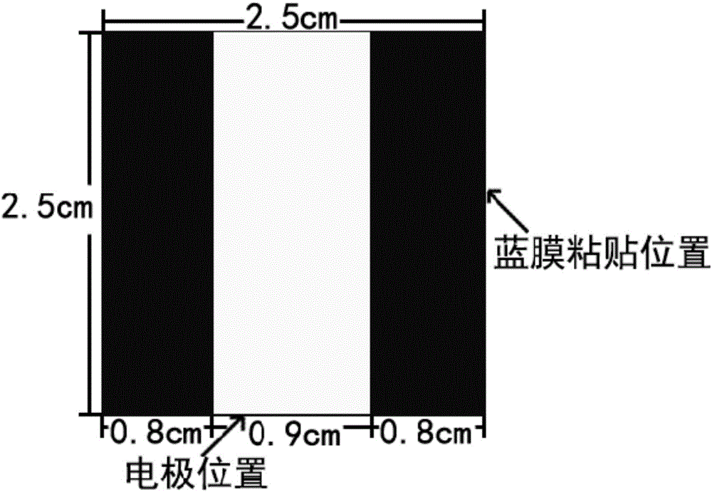
[0043] 1) Use the method mentioned in Example 1 to make silver nanowire electrodes, because OLED devices need to be made, so after step 2), you need to add a step, that is, stick a strip structure on both sides of the upper surface of the substrate near the edge. PVC blue film tape, and then spin coating, so that the silver nanowire film can only be spin-coated on the substrate in the middle area, so as to realize the preparation of strip electrodes, the position of the blue film paste and the shape of the electrode are as follows: image 3 shown. Since the samples that can be put in once are limited when preparing the OLED device, the best 15 minutes in Example 1 are selected for the treatment time of the plasma;

[0044] 2) Use an evaporation coating machine to make an OLED device. Th...


PUM

PropertyMeasurementUnit
diameteraaaaaaaaaa
lengthaaaaaaaaaa
thicknessaaaaaaaaaa

Abstract

The invention discloses a method of adopting plasma technology to treat silver nanowires and transferring through a substrate to prepare an organic photoelectronic device flexible electrode and belongs to the technical field of organic photoelectronics. The method includes: preparing a silver nanowire solution, spin-coating the silver nanowires on a silicon wafer to obtain a silver nanowire thin film, and treating the silver nanowire thin film through plasma, wherein PVP on the surfaces of the nanowires is removed, and surface appearance of the silver nanowires is changed; spin-coating photo-crosslinking polymer on the silicon wafer to complete cover the silver nanowire thin film, using an ultraviolet lamp to irradiate, and using a scalpel to separate the photo-crosslinking polymer from the silicon substrate to finally obtain a high-conductivity silver nanowire transparent electrode. By the method, surface roughness of the silver nanowire thin film is lowered while surface uniformity of the same is improved, the OLED flexible electrode obtained by the method is better than electrodes obtained through conventional thermal treatment methods in conductivity, and more time is saved.

Description

technical field [0001] The invention belongs to the technical field of organic optoelectronics, and in particular relates to a method for processing silver nanowires with plasma technology and preparing OLED flexible electrodes through substrate transfer. Background technique [0002] OLED (Organic Light Emitting Diode) has the advantages of high luminous efficiency, low driving voltage, fast response, rich colors, high contrast and large viewing angle, etc., and has excellent application prospects in the fields of lighting and flat panel display. Both the light-emitting layer and the carrier transport layer of OLED are made of organic materials, which have good bending properties. Therefore, whether flexible electrodes with good performance can be prepared has become the key to the development of flexible OLEDs. At present, the main electrode material for OLED industrial production is ITO (tin-doped indium oxide), which has high visible light transmittance and infrared refl...

Claims


Application Information

Patent Timeline
Patent Type & Authority Applications(China)
IPC IPC(8): H01L51/56
CPCH10K71/60H10K71/00
Inventor 段羽李俊陈平韦梦竹陶冶赵毅
Owner JILIN UNIV
Why Eureka
Try Eureka