Elastic circuit fabrication method based on metal sacrificial layer process

A technology of metal sacrificial layer and metal circuit, which is applied in the manufacture of printed circuits, removal of conductive materials by chemical/electrolytic methods, and printed circuits. Difficulty, simplification of the process flow, and the effect of overcoming the problems of metal wire cracks and open circuits

Inactive Publication Date: 2017-02-01
SHANGHAI JIAO TONG UNIV
View PDF5 Cites 12 Cited by
  • Summary
  • Abstract
  • Description
  • Claims
  • Application Information

AI Technical Summary

Problems solved by technology

However, the elastic circuit prepared based on this method has the problems of complex manufacturing process, difficulty in mass production, and the risk of dielectric leakage.

Method used


Image

  • Elastic circuit fabrication method based on metal sacrificial layer process
  • Elastic circuit fabrication method based on metal sacrificial layer process
  • Elastic circuit fabrication method based on metal sacrificial layer process

Examples


Embodiment 1

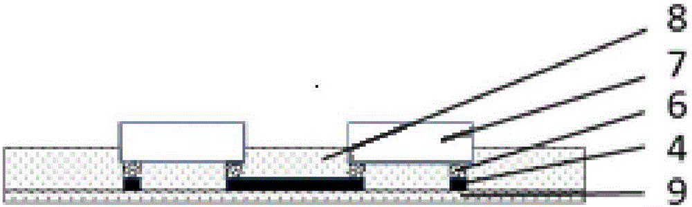
[0039] This embodiment relates to the preparation of elastic circuits based on the metal sacrificial layer technology and the prepared elastic circuits. The elastic circuit as figure 2 As shown, the material of the upper elastic polymer 8 is polydimethylsiloxane, and its thickness is 500 microns; the electronic component 7 is a single-chip microcomputer, a sensor or a capacitor resistor, etc.; the solder paste 6 is a low-temperature solder paste with a melting temperature of 130°C; The metal circuit and pad 4 are made of copper with a thickness of 10 microns and a line width of 100-4000 microns; the elastic polymer 9 of the lower layer is polydimethylsiloxane with a thickness of 100 microns.

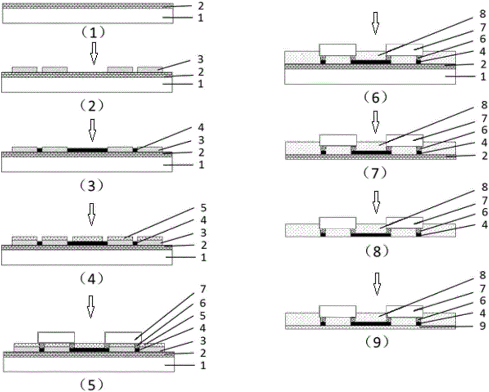
[0040] The elastic circuit preparation process based on the metal sacrificial layer process in this embodiment is as follows figure 1 As shown, including steps (1)-(9), specifically as follows:

[0041] (1) Make an aluminum thin film (metal thin film 2) and paste it on the glass subst...

Embodiment 2

[0061] The elastic circuit preparation based on the metal sacrificial layer process and the elastic circuit prepared in this embodiment are the same as in embodiment 1, except that the material of the upper elastic polymer 8 is elastic silicone rubber with a thickness of 50 microns; The circuit and the pad 4 are snake-shaped, the material is gold, the thickness is 1 micron, and the line width is 10-100 microns; the lower elastic polymer 9 is elastic silicone rubber, and the thickness is 50 microns; the substrate used is a silicon substrate , the metal film used is a copper film with a thickness of 15 microns.

Embodiment 3

[0063] The elastic circuit preparation based on the metal sacrificial layer process and the elastic circuit prepared in this embodiment are the same as in embodiment 1, except that the material of the upper elastic polymer 8 is polydimethylsiloxane, and its thickness is 300 microns; the metal circuit and pad 4 are S-shaped, the material is silver, the thickness is 50 microns, and the line width is 1000-4000 microns; the lower elastic polymer 9 is elastic silicone rubber, and the thickness is 500 microns; the substrate used As the ceramic sheet substrate, the metal film used is an aluminum film with a thickness of 200 microns.


PUM


Abstract

The invention discloses an elastic circuit fabrication method based on a metal sacrificial layer process. The elastic circuit fabrication method comprises the following steps of pasting a metal thin film on a substrate; spin-coating photoresist on a surface of the metal thin film, and photoetching a circuit and bonding pad layout; fabricating metal circuits and bonding pads on a circuit and bonding pad layout region, spin-coating photosensitive organic soluble polymers, and photoetching a soldering mask layout; welding electronic components on the bonding pads; removing the photoresist and the photosensitive organic soluble polymers, casting an upper-layer elastic polymer and curing the upper-layer elastic polymer; stripping the metal thin film and an upper-layer structure thereof from the substrate; etching the metal thin film; and spin-coating and curing a lower-layer elastic polymer. By the elastic circuit fabrication method, a metal seed layer is not needed to be deposited, and the problem of metal wire crack or open circuit caused by different matching of the elastic polymers and metal heat is thoroughly solved; and meanwhile, a stress buffer layer is omitted, the process flow is simplified, only processes of photoetching, electroplating and etching are needed, and the elastic circuit fabrication method has the advantages of high yield, simplicity in welding and compatibility of a reflow soldering process.

Description

technical field [0001] The invention relates to the technical field of circuit preparation, in particular to a method for preparing an elastic circuit based on a metal sacrificial layer technology. Background technique [0002] Common rigid electronic devices such as printed circuit boards (PCB) have the disadvantages of being unable to bend and stretch, unable to form a tight fit with curved surfaces, and not suitable for moving parts (such as human elbow joints, robot joints). In addition, when rigid electronic devices are used in the wearable field, because they cannot be tightly attached to the skin surface, the measurement errors of sensors (such as heart rate and EEG sensors) become larger, and there are disadvantages of uncomfortable wearing and unsuitable for long-term wearing. Electronic devices based on elastic material substrates can well overcome the shortcomings of electronic devices based on rigid substrates, so they have gradually attracted the attention of re...

Claims


Application Information

Patent Timeline
Patent Type & Authority Applications(China)
IPC IPC(8): H05K3/00H05K3/06H05K3/34
CPCH05K3/06H05K3/0014H05K3/34H05K2203/1453
Inventor 陈迪林树靖彼得·布兰得利·沙尔徐俊凯仇三铭韦黔崔大祥
Owner SHANGHAI JIAO TONG UNIV
Why Eureka
Try Eureka