SOI substrate-based La-based high-dielectric constant gate dielectric structure and manufacturing method thereof

A high-dielectric-constant, high-dielectric-constant material technology, applied in nanotechnology, circuits, electrical components, etc. for materials and surface science, can solve problems that do not conform to the development of the thermal budget of the semiconductor industry and the poor step coverage of gate dielectrics. It can reduce the mobility of sodium ions, improve the anti-radiation performance, and improve the performance of the film.

Inactive Publication Date: 2017-03-15
XIDIAN UNIV
View PDF2 Cites 0 Cited by
  • Summary
  • Abstract
  • Description
  • Claims
  • Application Information

AI Technical Summary

Problems solved by technology

[0005] On the other hand, as the traditional metal oxide deposition process, metal organic compound chemical vapor deposition MOCVD, molecular beam epitaxy growth MBE and other processes grow the gate dielectric step coverage is not good, and the surface roughness is large, resulting in poor film interface quality. Not good, this will seriously affect the overall quality of the film, thereby affecting the reliability of the device, and its higher growth temperature does not conform to the trend of the semiconductor industry towards lower thermal budget

Method used


Image

  • SOI substrate-based La-based high-dielectric constant gate dielectric structure and manufacturing method thereof
  • SOI substrate-based La-based high-dielectric constant gate dielectric structure and manufacturing method thereof
  • SOI substrate-based La-based high-dielectric constant gate dielectric structure and manufacturing method thereof

Examples


example 1

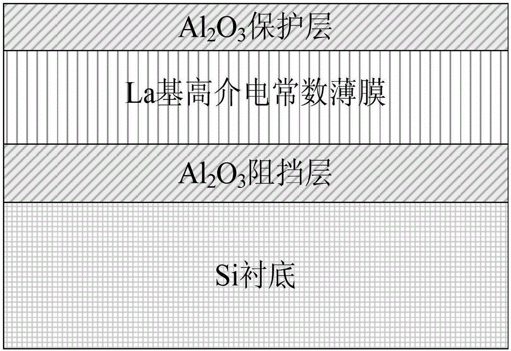
[0033] Example 1, Preparation of Al 2 O 3 \La 2 O 3 \Al 2 O 3 \SOI structure of high dielectric constant material gate dielectric.

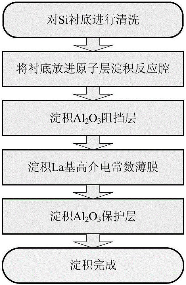
[0034] Step 1. Clean the SOI substrate.

[0035] 1a) Soak the SOI substrate in the SC-1 solution heated to 75℃ for 10 minutes. The composition of the solution is NH 4 OH, H 2 O 2 And H 2 O, the ratio is 5:1:1, used to remove organic pollutants or attached particles on the SOI substrate;

[0036] 1b) Rinse the soaked SOI substrate in deionized water for 2 minutes to remove the residual SC-1 solution, and then take it out;

[0037] 1c) Wash the SOI substrate in an HF solution for 60 seconds before taking it out. The components of the solution are HF and H 2 O, the ratio is 1:50. The main function of this cleaning is to remove the natural oxide layer SiO on the surface of the SOI substrate 2 ;

[0038] 1d) Rinse the SOI substrate in deionized water to remove the residual HF solution, and then take it out;

[0039] 1e) Put the SOI substrate in deionized water a...

example 2

[0060] Example 2, Preparation of Al 2 O 3 \LaAlO 3 \Al 2 O 3 \SOI structure of high dielectric constant material gate dielectric.

[0061] Step one, cleaning the SOI substrate.

[0062] The specific implementation of this step is the same as step 1 of Example 1.

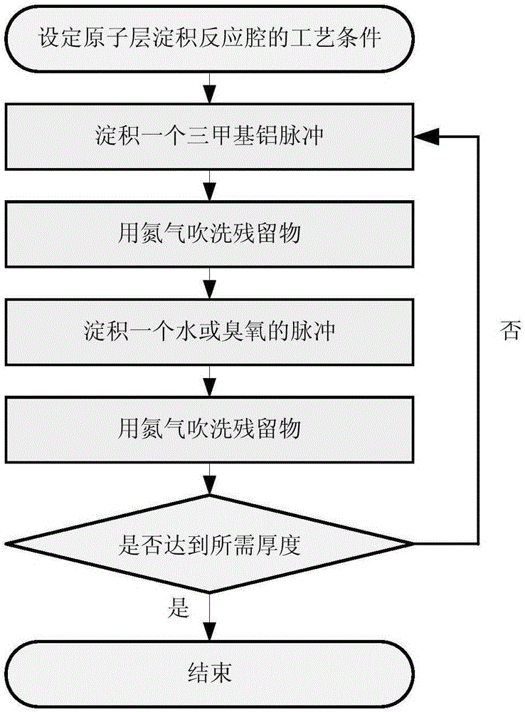
[0063] Step 2: Put the cleaned SOI substrate into the reaction chamber of the atomic layer deposition equipment, and deposit Al on the blow-dried substrate using the atomic layer deposition method 2 O 3 Barrier layer.

[0064] Reference image 3 , The specific implementation of this step is as follows:

[0065] 2.1) Evacuate the pressure of the atomic layer deposition equipment cavity to 12hPa, heat the temperature to 350°C, and set the nitrogen flow rate for purging to 250sccm;

[0066] 2.2) Deposit a pulse of trimethylaluminum for 0.3 seconds on the SOI substrate, such as Figure 5 As shown in t1, Al-O-Al-CH is generated 3 *And CH 4 ;

[0067] 2.3) Use nitrogen to treat the trimethylaluminum that was not successfully deposite...

example 3

[0084] Example 3. Preparation of Al 2 O 3 \HfLaO\Al 2 O 3 \SOI structure of high dielectric constant material gate dielectric

[0085] Step A, cleaning the SOI substrate.

[0086] The specific implementation of this step is the same as step 1 of Example 1.

[0087] Step B: Put the cleaned SOI substrate into the reaction chamber of the atomic layer deposition equipment, and deposit Al on the blow-dried substrate using the atomic layer deposition method 2 O 3 Barrier layer.

[0088] Reference image 3 , The specific implementation of this step is as follows:

[0089] B1) Evacuate the pressure of the atomic layer deposition equipment cavity to 20hPa, heat the temperature to 300°C, and set the nitrogen flow rate for purging to 200sccm;

[0090] B2) Deposit a pulse of trimethylaluminum for 0.1 second on the SOI substrate, such as Figure 5 As shown in t1, Al-O-Al-CH is generated 3 *And CH 4 ;

[0091] B3) Use nitrogen to treat the trimethylaluminum that was not successfully deposited on the S...


PUM

PropertyMeasurementUnit
thicknessaaaaaaaaaa
thicknessaaaaaaaaaa
thicknessaaaaaaaaaa

Abstract

The invention discloses an SOI substrate-based high-dielectric constant gate dielectric material, and aims at mainly solving the problems of a low dielectric constant, poor heat stability and thin film compactness and the like of an existing gate dielectric material. The gate dielectric material comprises an SOI substrate (1), a barrier layer (2), an La-based high-dielectric constant thin film (3) and a protective layer (4) from bottom to top, wherein Al2O3 of which the thickness is 0.5-4nm is adopted by the barrier layer (2); La2O3 or LaAlO3 or HfLaOx of which the thickness is 1-10nm is adopted by the La-based high-dielectric constant thin film (3); and Al2O3 of which the thickness is 1-4nm is adopted by the protective layer (4). The whole gate dielectric is prepared by adopting an atomic layer deposition method and the technology is compatible with an existing CMOS technology. The SOI substrate-based high-dielectric constant gate dielectric material has the advantages of a high dielectric constant, good thin film compactness and step coverage, good heat stability and small surface roughness, and can be used for manufacturing of a metal oxide semiconductor field effect transistor.

Description

Technical field [0001] The invention belongs to the technical field of semiconductor materials, and particularly relates to a La-based high-dielectric constant gate dielectric structure based on an SOI substrate and a manufacturing method thereof, which can be used for manufacturing a gate dielectric film of a metal oxide semiconductor field effect transistor. Background technique [0002] With the continuous development of microelectronics technology, the research and development of high-performance and integrated multi-function ICs has higher and higher requirements for materials. Silicon-on-insulator SOI materials are new types of integrated circuit materials, which are praised by many scholars as "the new type of 21st century Silicon-based integrated circuit technology". Compared with bulk silicon, SOI has the advantages of no latch, high speed, low voltage, low power consumption and radiation resistance. In addition, the requirement for high integration has continuously red...

Claims


Application Information

Patent Timeline
Patent Type & Authority Applications(China)
IPC IPC(8): H01L29/423H01L29/51H01L21/285B82Y30/00
CPCH01L29/42364B82Y30/00H01L21/285H01L29/401H01L29/513H01L29/517
Inventor 刘红侠冯兴尧汪星刘贺蕾赵璐费晨曦
Owner XIDIAN UNIV
Why Eureka
Try Eureka