Organic light-emitting display device

A light-emitting display device, an organic technology, applied in the direction of electric solid-state devices, electrical components, circuits, etc., can solve the problems of high requirements for the main material, comparable, and failure to reach the commercialization of OLEDs

Inactive Publication Date: 2017-06-06
AAC TECH NANJING
View PDF7 Cites 7 Cited by
  • Summary
  • Abstract
  • Description
  • Claims
  • Application Information

AI Technical Summary

Problems solved by technology

[0009] 1. Low quantum efficiency
Low quantum efficiency is the fatal shortcoming of traditional fluorescent light-emitting devices
Since traditional fluorescent light-emitting devices can only utilize only 25% of S 1 Excitons undergo fluorescence emission, which makes it difficult for the external quantum efficiency of existing fluorescent light-emitting devices to be comparable to that of phosphorescent light-emitt

Method used


Image

  • Organic light-emitting display device
  • Organic light-emitting display device
  • Organic light-emitting display device

Examples


Embodiment 1

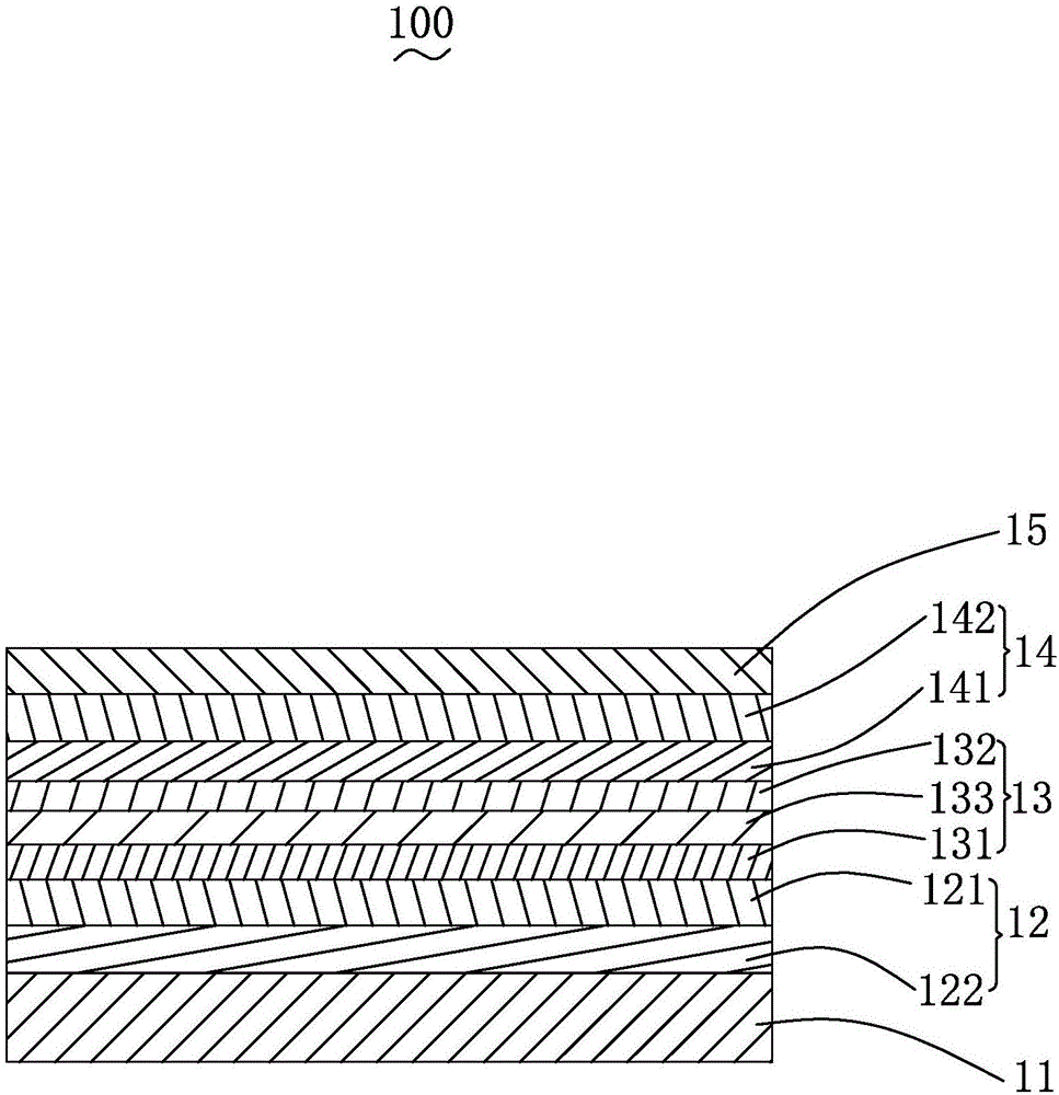
[0089] see figure 1 , is a schematic structural view of Embodiments 1-4 of the organic light-emitting display device provided by the present invention. The organic light emitting display device 100 includes a first conductive layer 11 , a hole transport part 12 , a light emitting layer 13 , an electron transport part 14 and a second conductive layer 15 which are sequentially deposited.

[0090] The first conductive layer 11 is an anode, and its material is ITO, IGZO, IZO, graphene, nano-silver wire, carbon nanotube and other materials; preferably ITO. The second conductive layer 15 is a cathode, and its material is a low work function metal or metal alloy, such as Al, Mg:Ag alloy or Ag, preferably Al.

[0091] The hole transport portion 12 includes a hole injection layer 121 and a hole transport layer 122 deposited on the hole injection layer 121, and the hole injection layer 121 is disposed between the first conductive layer 11 and the Between the hole transport layer 122. ...

Embodiment 2

[0155] combine figure 1 And the specific materials of each layer structure,

[0156] The structure of Example 2 is: ITO / NPB / TCTA / TCTA:PdN3N:DCM1 / TCTA / TCTA:PdN3N:DCM1 / TPBi / Bphen / LiF / Al.

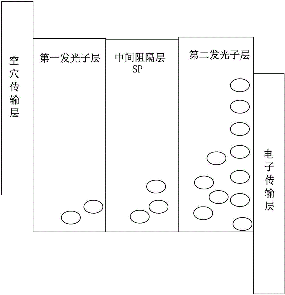
[0157] Both the first luminescent sublayer 131 and the second luminescent sublayer 132 are formed by doping a metal-assisted delayed fluorescence sensitizer, a host material, and a fluorescent guest material. The first luminescent sublayer 131 and the second luminescent sublayer 131 The middle barrier layer 133 is formed between the luminescent sub-layers 132 .

[0158] In the first luminescent sublayer 131 and the second luminescent sublayer, PdN3N is used as a metal-assisted delayed fluorescence sensitizer, TCTA is used as a host material, and DCM1 is used as a fluorescent guest material, which belongs to a red fluorescent material with a CIE (0.64 , 0.34).

[0159] Please refer to Figure 6 , Figure 7 ,in Figure 6 It is the absorption spectrum and emission spectrum diagram of PdN3N;...

Embodiment 3

[0165] combine figure 1 And the specific materials of each layer structure,

[0166] The structure of Example 3 is: ITO / NPB / TCTA / TCTA:PdN3N:DCJTB / TCTA / TCTA:PdN3N:DCJTB / TPBi / Bphen / LiF / Al.

[0167] Both the first luminescent sublayer 131 and the second luminescent sublayer 132 are formed by doping a metal-assisted delayed fluorescence sensitizer, a host material, and a fluorescent guest material. The first luminescent sublayer 131 and the second luminescent sublayer 131 The middle barrier layer 133 is formed between the luminescent sub-layers 132 .

[0168] Please combine Figure 6 and Figure 9 ,in Figure 9 It is the absorption spectrum figure of DCJTB, wherein curve a represents the fluorescence intensity curve of Alq (Alq represents 3,8-hydroxyquinoline aluminum), curve b represents the absorption intensity curve of DCJTB, and curve c represents the absorption intensity curve of QAD (QAD represents quinoline Acridine (two) ketone), curve d represents the fluorescence in...


PUM

PropertyMeasurementUnit
Thicknessaaaaaaaaaa

Abstract

The invention discloses an organic light-emitting display device. The organic light-emitting display device includes a first conducting layer, a second conducting layer, a hole transport part and an electron transport part which are formed between the first conducting layer and the second conducting layer and a luminous layer formed between the hole transport part and the electron transport part, and is characterized in that the luminous layer includes n+1 layers of luminous sublayers and intermediate barrier layers formed between two adjacent luminous sublayers, and at least one of the luminous sublayers is formed by doping a metal auxiliary delayed fluorescent sensitizer, a host material and a fluorescent guest material, wherein n is a natural number larger than or equal to 1. The organic light-emitting display device provided by the invention can transfer 100% of exciton energy to the fluorescent guest material to perform fluorescence radiation, thereby improving the luminous efficiency.

Description

[0001] 【Technical field】 [0002] The invention relates to the technical field of light emitting diodes, in particular to an organic light emitting display device. [0003] 【Background technique】 [0004] An organic light-emitting diode (Organic Light-Emitting Diode, OLED) device can be used as a light source for a display device and an illumination device, and has the advantages of wide viewing angle, short response time, thinness and arbitrary bending. [0005] For the convenience of description, the English abbreviations of each layer structure in the organic light-emitting display device will be described, HIL means hole injection layer, HTL means hole transport layer, EML means light emitting layer, ETL means electron transport layer, EIL means electron injection layer. The light-emitting mechanism of OLED is that when a bias voltage is applied to the OLED device, holes are injected from the anode, transition to the EML via HIL / HTL, electrons are injected from the cathode...

Claims


Application Information

Patent Timeline
IPC IPC(8): H01L51/50
CPCH10K50/11H10K50/121
Inventor 谢再锋
Owner AAC TECH NANJING
Why Eureka
Try Eureka