Production method of nitride epitaxial wafers and gallium nitride laser device

A growth method and epitaxial wafer technology, applied in the field of optoelectronics, can solve problems such as poor quality of nitride materials, inability to grow AlN layers, poor film quality, etc., achieve stress reduction, good thickness controllability, and solve lattice mismatch Effect

Active Publication Date: 2017-06-20
INST OF ELECTRONICS ENG CHINA ACAD OF ENG PHYSICS
View PDF8 Cites 9 Cited by
  • Summary
  • Abstract
  • Description
  • Claims
  • Application Information

AI Technical Summary

Problems solved by technology

However, the disadvantages of this method still exist: using magnetron sputtering, the sputtering speed is fast, but the quality of the film is poor, there are many impurities, and further heat treatment is required after the film is grown by sputtering, so this method cannot Growth of better AlN layers results in poorer quality nitride materials obtained

Method used


Image

  • Production method of nitride epitaxial wafers and gallium nitride laser device
  • Production method of nitride epitaxial wafers and gallium nitride laser device

Examples


Embodiment 1

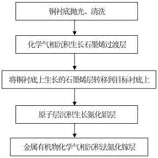
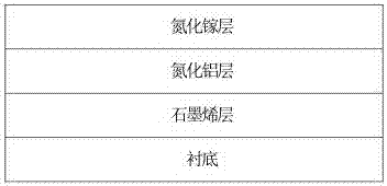
[0049] In step S1, the copper substrate is cleaned to remove the oil stain and oxide layer on the surface, and after double polishing of mechanical polishing and electrochemical polishing, it is washed with ethanol and deionized water three times in sequence, washed with dilute hydrochloric acid for 5-10 minutes, and washed with deionized water. several times, N 2 Blow dry to get copper substrate.

[0050] Step S2 grows a graphene layer on the copper substrate:

[0051] S2a Put the copper substrate treated in step S1 into the quartz tube of tube furnace, and vacuumize for 5 minutes;

[0052] S2b injects hydrogen, heats the tube furnace to 800°C and anneals for 1 hour;

[0053] In S2c, the carbon source gas methane and the mixed gas of argon and hydrogen with a volume ratio of 10:1 are introduced to grow, the carbon source gas methane and hydrogen are turned off, and the quartz tube of the tube furnace is cooled to room temperature with the furnace in an argon atmosphere to obt...

Embodiment 2

[0067] In step S1, the copper substrate is cleaned to remove the oil stain and oxide layer on the surface, and after double polishing of mechanical polishing and electrochemical polishing, it is washed with ethanol and deionized water three times in sequence, washed with dilute hydrochloric acid for 5-10 minutes, and washed with deionized water. several times, N 2 Blow dry to get copper substrate.

[0068] Step S2 grows a graphene layer on the copper substrate:

[0069] S2a Put the copper substrate treated in step S1 into the quartz tube of tube furnace, and vacuumize for 5 minutes;

[0070] S2b is fed with hydrogen, the flow rate is 100 sccm, and the tube furnace is heated to 1000°C and then annealed for 2 hours;

[0071] In S2c, the carbon source gas methane and the mixed gas of argon and hydrogen with a volume ratio of 20:1 are introduced to grow, the carbon source gas methane and hydrogen are closed, and the quartz tube of the tube furnace is cooled to room temperature u...

Embodiment 3

[0084] In step S1, the copper substrate is cleaned to remove the oil stain and oxide layer on the surface, and after double polishing of mechanical polishing and electrochemical polishing, it is washed with ethanol and deionized water three times in sequence, washed with dilute hydrochloric acid for 5-10 minutes, and washed with deionized water. several times, N 2 Blow dry to get copper substrate.

[0085] Step S2 grows a graphene layer on the copper substrate:

[0086] S2a Put the copper substrate treated in step S1 into the quartz tube of tube furnace, and vacuumize for 7 minutes;

[0087] S2b is fed with hydrogen, the flow rate is 100 sccm, and the tube furnace is heated to 1050°C and then annealed for 3 hours;

[0088] In S2c, the carbon source gas methane and the mixed gas of argon and hydrogen with a volume ratio of 20:1 are introduced to grow, the carbon source gas methane and hydrogen are closed, and the quartz tube of the tube furnace is cooled to room temperature u...


PUM

PropertyMeasurementUnit
thicknessaaaaaaaaaa
thicknessaaaaaaaaaa

Abstract

The invention relates to a production method of nitride epitaxial wafers and a gallium nitride laser device. The method comprises the following steps that 1, a copper substrate is polished and cleaned; 2, a graphene layer grows on the copper substrate; 3, the graphene layer growing on the copper substrate is transferred to target substrates; 4, an aluminum nitride thin layer grows on the graphene layer through an atomic layer deposition method; and 5, a GaN layer grows on the aluminum nitride thin layer through a metal organic matter chemical vapor deposition method. By means of the method, the nitride epitaxial wafers can grow on the different target substrates, the epitaxial wafers are transferred through the copper substrate, and therefore graphene is transferred to the different target substrates. The graphene layer is used as a buffer layer between the substrate and the GaN epitaxial layer, and the aluminum nitride layer is prepared through the atomic layer deposition method. Layer-by-layer growth of material atomic layers, good thickness controllability and high-precision film growth quality can be achieved, the large lattice mismatch problem between the substrate and the epitaxial layer is solved, the epitaxial layer quality is improved, and high-quality gallium nitride laser device can be obtained.

Description

technical field [0001] The invention relates to a growth method of a nitride epitaxial wafer and a gallium nitride laser, belonging to the field of optoelectronic technology. Background technique [0002] GaN material has received more and more attention as a new type of semiconductor material. As a representative material of the third-generation semiconductor, gallium nitride has excellent electrical and optical properties. It has the advantages of wide bandgap, direct bandgap, high temperature and high pressure resistance, and high electron mobility. It is used in the fields of electronic devices and optoelectronic devices. It has a wide range of applications, so the preparation of high-quality gallium nitride is the key to the preparation of the above devices. [0003] Graphene is a new two-dimensional nanomaterial whose atoms are linked together by sp2 electron orbitals, and because graphene has a hexagonal close-packed atomic lattice, which is the same as the arrangeme...

Claims


Application Information

Patent Timeline
Patent Type & Authority Applications(China)
IPC IPC(8): C23C16/26C23C16/34C23C16/01C23C16/455H01S5/323
CPCC23C16/01C23C16/26C23C16/303C23C16/45525H01S5/323
Inventor 王文杰龙衡李俊泽李沫张健
Owner INST OF ELECTRONICS ENG CHINA ACAD OF ENG PHYSICS
Why Eureka
Try Eureka