
A kind of znse nano wire and its preparation method and application

A nanowire and substrate technology, applied in nanotechnology, nanotechnology, nanotechnology for materials and surface science, etc., can solve problems such as limiting practical applications, affecting the physical and chemical properties of nanowires, and achieving good crystallinity. Effect

Active Publication Date: 2019-03-19
THE NAT CENT FOR NANOSCI & TECH NCNST OF CHINA
View PDF1 Cites 0 Cited by
  • Summary
  • Abstract
  • Description
  • Claims
  • Application Information

AI Technical Summary

Problems solved by technology

However, for face-centered cubic crystals with sphalerite structure, a large number of stacking fault defects are easily formed inside the nanowires grown along the , and crystal directions.
The existence of these stacking fault defects will seriously affect the physicochemical properties of nanowires, thereby limiting their practical applications.

Method used


Image

  • A kind of znse nano wire and its preparation method and application
  • A kind of znse nano wire and its preparation method and application
  • A kind of znse nano wire and its preparation method and application

Examples


preparation example Construction

[0064] Preferably, the preparation method of the ZnSe nanowires comprises the following steps:

[0065] (1) With FTO conductive glass or SnO 2 A single crystal substrate is used as a substrate, and a gold film is deposited on the surface of the substrate;

[0066] (2) step (1) is deposited with the substrate of gold film in vacuum calcining;

[0067] (3) placing the substrate calcined in step (2) and the quartz boat equipped with ZnSe powder in the large quartz tube of the dual-temperature zone tube furnace;

[0068] (4) evacuate the tube furnace described in step (3), feed protective gas simultaneously, heat the temperature zone that substrate and quartz boat are respectively housed respectively, cool naturally after the same time of insulation, on the substrate Obtain ZnSe nanowires.

Embodiment 1

[0071] The process of preparing ZnSe nanowires is as follows:

[0072] (1) Use isopropanol, acetone, and ethanol to ultrasonically clean the FTO conductive glass substrate in sequence;

[0073] (2) Deposit a 0.5nm thick gold film on the surface of the FTO conductive glass substrate as the catalyst required for ZnSe nanowire growth;

[0074] (3) Calcining the FTO conductive glass substrate deposited with the gold film at 540° C. for 30 min in a vacuum;

[0075] (4) 35mg ZnSe powder is packed in the quartz boat, the quartz boat that ZnSe powder is housed and the FTO conductive glass substrate that is deposited with gold film through calcining process are put into the large quartz tube of double-temperature zone tubular furnace, Adjust the positions of the quartz boat and the substrate to be in the center of the first temperature zone and the second temperature zone of the tube furnace;

[0076] (5) Connect the tube furnace, turn on the vacuum pump, evacuate from the side of th...

Embodiment 2

[0085] The process of preparing ZnSe nanowires is as follows:

[0086] (1) Ultrasonic cleaning of SnO with isopropanol, acetone, and ethanol in sequence 2 Single crystal substrate;

[0087] (2) to SnO 2 A 0.5nm thick gold film is deposited on the surface of the single crystal substrate as the catalyst required for the growth of ZnSe nanowires;

[0088](3) SnO deposited with a gold film 2 The single crystal substrate was calcined at 530°C for 28min in vacuum;

[0089] (4) 20mg ZnSe powder is packed into a quartz boat, and the quartz boat equipped with ZnSe powder and the SnO deposited with a gold film through calcination 2 Put the single crystal substrate into the large quartz tube of the dual temperature zone tube furnace, adjust the positions of the quartz boat and the substrate to be in the center of the first temperature zone and the second temperature zone of the tube furnace respectively;

[0090] (5) Connect the tube furnace, turn on the vacuum pump, evacuate from t...


PUM

PropertyMeasurementUnit
thicknessaaaaaaaaaa
diameteraaaaaaaaaa
lengthaaaaaaaaaa

Abstract

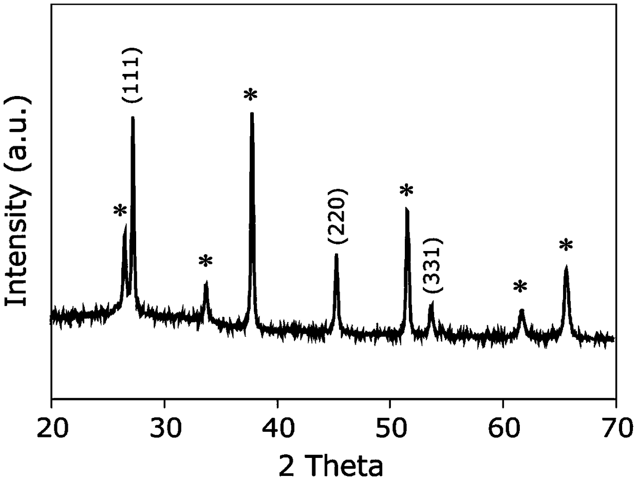
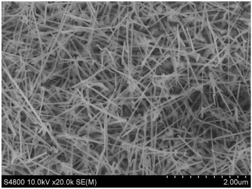
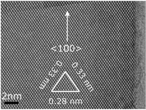
The invention relates to a ZnSe nanowire and a preparation method and an application thereof. The ZnSe nanowire is grown along the crystal orientation of the <100>. The ZnSe nanowire is provided with a sphalerite structure, the average diameter is 20 nm-80 nm, the length is 0.5 [mu]m-10 [mu]m, the size is uniform, the crystallinity is good, and the ZnSe nanowire has no structural defects such as a stacking fault. According to the ZnSe nanowire and the preparation method and the application thereof, ZnSe powder servers as pre-reaction materials, gold serves as a catalyst, and the ZnSe nanowire growing is obtained through growth on FTO conductive glass or a SnO2 single crystal substrate by a chemical vapor deposition method. The nanowire can be used for constructing solar batteries, photodetectors, nanometer lasers and the like, performance is especially good in the aspect of hydrogen production through solar photoelectrocatalysis decomposition of water, and good application prospects are achieved.

Description

technical field [0001] The invention relates to the field of semiconductor materials and nanotechnology, in particular to a ZnSe nanowire and its preparation method and application. Background technique [0002] One-dimensional nanostructured materials have special properties that many macroscopic materials do not have due to their small geometric size and shape anisotropy, and have shown great promise in optics, electronics, magnetism and other physical and chemical fields. Therefore, the controllable preparation of one-dimensional nanostructures of various semiconductor materials has become a research hotspot in the field of materials science today. [0003] Zinc selenide (ZnSe) is an important II-VI semiconductor material because of its large band gap (2.7eV), large light transmission range (0.5-22μm), high luminous efficiency and comparative Low absorption coefficient, considered to be an ideal candidate material for constructing optoelectronic devices such as blue-gree...

Claims


Application Information

Patent Timeline
Patent Type & Authority Patents(China)
IPC IPC(8): C23C16/30C23C16/02C25B1/04C03C17/34B82Y30/00B82Y40/00
CPCB82Y30/00B82Y40/00C03C17/3411C03C2218/152C23C16/0281C23C16/306C25B1/04C25B1/55Y02E60/36
Inventor 亚瑟·阿巴斯张凯宫建茹
Owner THE NAT CENT FOR NANOSCI & TECH NCNST OF CHINA
Learn More