Front surface grid-line-free P type crystal silicon back contact two-sided battery structure and manufacturing method therefor

A double-sided cell and front-side grid line technology, applied in the field of solar cells, can solve the problems of MWT battery leakage problems, reduce the production cost of cells, and not be applied on a large scale, so as to prevent leakage and improve conversion Efficiency, the effect of reducing production costs

Active Publication Date: 2017-08-01
滁州隆基乐叶光伏科技有限公司
View PDF5 Cites 12 Cited by
  • Summary
  • Abstract
  • Description
  • Claims
  • Application Information

AI Technical Summary

Problems solved by technology

Although the MWT battery technology reduces the light-shielding area of ​​the main grid electrode on the front of the battery, the thin grid lines on the front of the battery still have about 3% of the light-shielding area. The thin grid lines are usually made of expensive silver, which is important for reducing the production cost of the battery sheet. unfavorable
In addition, the leakage problem of MWT battery has not been solved well
The above problems make MWT, as the core technology for improving the front of the battery, has not been applied on a large scale.

Method used


Image

  • Front surface grid-line-free P type crystal silicon back contact two-sided battery structure and manufacturing method therefor
  • Front surface grid-line-free P type crystal silicon back contact two-sided battery structure and manufacturing method therefor
  • Front surface grid-line-free P type crystal silicon back contact two-sided battery structure and manufacturing method therefor

Examples


Embodiment 1

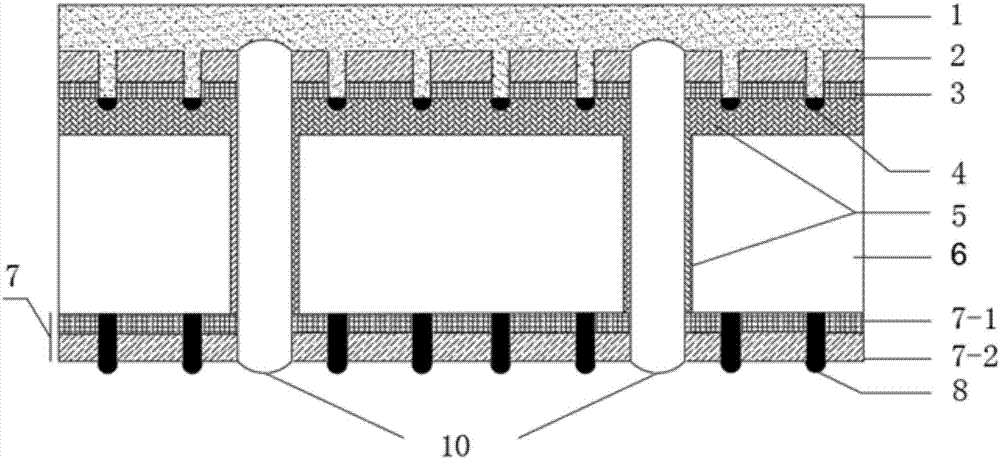
[0078] (1) On the P-type single crystal silicon wafer, 5×5 through holes arranged equidistantly are formed by laser, and the diameter of a single through hole is 300um.

[0079] (2) Anisotropic etching of the P-type monocrystalline silicon wafer after making through holes in a KOH solution at about 80°C to obtain a pyramid structure on the surface.

[0080] (3) Use POCl at 800-900°C 3 The dopant is diffused under low pressure, and an N-type layer is formed on the front surface of the silicon wafer and the surface layer of the through-hole wall. The square resistance after doping is 20Ω / □.

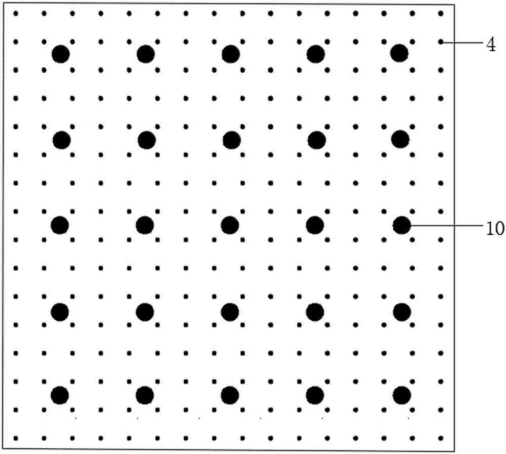
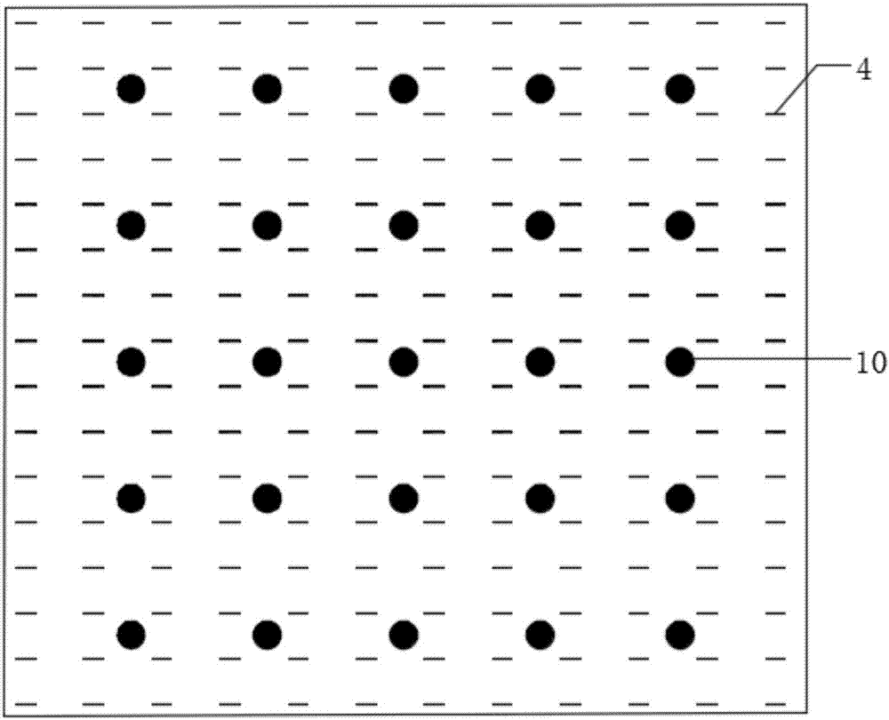
[0081] (4) Spray paraffin wax on the N-type layer according to the array pattern and through holes by inkjet method as a mask. The array pattern is a dot array, the diameter of a single dot is 50um, and the distance between dots is 0.8mm.

[0082] (5) Use wet etching to remove the phosphosilicate glass, back knot and paraffin on the front side of the silicon wafer. A heavy doping is form...

Embodiment 2

[0090] (1) On the P-type polysilicon wafer, 6×6 through holes arranged equidistantly are formed by laser, and the diameter of a single through hole is 200um.

[0091] (2) Put the P-type polysilicon wafer with through-holes in dry plasma texturing equipment to obtain multi-shaped micro-nano structures, and then perform surface modification in BOE solution.

[0092] (3) by pH 3 As the impurity, it is doped by ion implantation, and then annealed to form an N-type layer on the front surface of the silicon wafer and the surface layer of the through-hole wall. The square resistance after doping is 30Ω / □.

[0093] (4) Spray paraffin wax on the N-type layer according to the array pattern and through holes by inkjet method as a mask. The array pattern is a line segment array, the length of the line segment is 1.5mm, the width is 100um, and the distance between the line segments is 2mm.

[0094] (5) Use wet etching to remove the phosphosilicate glass, back knot and paraffin on the fro...

Embodiment 3

[0102] (1) On the P-type single crystal silicon wafer, 5×5 through holes arranged equidistantly are formed by laser, and the diameter of a single through hole is 400um.

[0103] (2) Put the P-type single crystal silicon wafer after making the through hole in the Cu(NO 3 ) 2 / H 2 o 2 Anisotropic etching was carried out in / HF solution to obtain an inverted pyramid structure on the surface.

[0104] (3) Use POCl at 800-900°C 3 The dopant is diffused under low pressure, and an N-type layer is formed on the front surface of the silicon wafer and the surface layer of the through-hole wall.

[0105] (4) Spray paraffin in the through hole by inkjet method as a mask.

[0106] (5) Use wet etching to remove the phosphosilicate glass, back knot and paraffin on the front side of the silicon wafer.

[0107] (6) Deposit 20nm aluminum oxide and 50nm silicon nitride successively on the back of the silicon wafer by PECVD method; deposit 20nm silicon oxide and 60nm silicon nitride success...


PUM


Abstract

The invention discloses a front surface grid-line-free P type crystal silicon back contact two-sided battery structure and a manufacturing method therefor. A transparent conductive film is positioned on a front surface passivation film and an antireflection film; via hole electrodes used for connecting front surface and back surface negative electrodes of the battery are arranged in through holes in a P type crystal silicon wafer; partial heavily-doped N+ regions distributed based on regular patterns are arranged on the surface layer of an N type layer; the transparent conductive film passes through the antireflection film and the front surface passivation film to be in electrical contact with the partial heavily-doped N+ regions and the top ends of the via hole electrodes to form a battery negative electrode; the transparent conductive film is used for guiding electrons collected on the front surface of the battery to the back surface of the battery through the via hole electrodes; and back surface positive electrode thin grid lines pass through a first back surface passivation film and a second back surface passivation film to form partial ohmic contact with a P type substrate and to be connected with back surface positive electrode main grid lines together to form a battery positive electrode. By virtue of the battery structure and the manufacturing method therefor, light shielding of the battery positive electrode is avoided, power output is increased, consumption amount of silver paste in the battery manufacturing process is reduced, and production cost is lowered.

Description

technical field [0001] The invention belongs to the technical field of solar cells, and in particular relates to a P-type crystalline silicon back-contact double-sided cell structure and a manufacturing method without front grid lines. Background technique [0002] Since the first solar cell was born in Bell Laboratories in 1954, crystalline silicon solar cells have been widely used, the conversion efficiency has been continuously improved, and the production cost has continued to decline. At present, crystalline silicon solar cells account for more than 90% of the global market for solar cells, and the conversion efficiency of crystalline silicon cell production lines has exceeded 21%. The cost of electricity continues to shrink and is expected to be flat in the next few years. As a clean energy source, crystalline silicon solar cells play an increasingly important role in changing the energy structure and alleviating environmental pressure. [0003] Due to the mature pro...

Claims


Application Information

Patent Timeline
Patent Type & Authority Applications(China)
IPC IPC(8): H01L31/0224H01L31/0216H01L31/042H01L31/18
CPCH01L31/02168H01L31/02245H01L31/042H01L31/1804Y02E10/50Y02P70/50
Inventor 赵科雄
Owner 滁州隆基乐叶光伏科技有限公司
Why Eureka
Try Eureka