Resin composition, and insulating film and semiconductor device using same

A technology of resin composition and insulating film, which is applied in the direction of electrical components, printed circuits, circuit substrate materials, etc., can solve the problems of toxic hydrofluoric acid, etc., and achieve the effect of good adhesive strength

Active Publication Date: 2017-08-18
NAMICS CORPORATION
View PDF9 Cites 6 Cited by
  • Summary
  • Abstract
  • Description
  • Claims
  • Application Information

AI Technical Summary

Problems solved by technology

In addition, since treatment at high temperature is required, there is a problem that toxic hydrofluoric acid may be generated due to the decomposition of fluororesin.

Method used


Image

  • Resin composition, and insulating film and semiconductor device using same
  • Resin composition, and insulating film and semiconductor device using same
  • Resin composition, and insulating film and semiconductor device using same

Examples


Embodiment 1~14

[0134] (Examples 1-14, Comparative Examples 1-5)

[0135]Sample Preparation and Assay Methods

[0136] After measuring and mixing each component so that the mixing ratio (parts by mass) shown in the table below was added, toluene was added, and the above-mentioned material was placed in a reaction vessel heated to 80° C., and the mixture was rotated at 150 rpm for 3 minutes. Hours of atmospheric mixing. Subsequently, the resin composition was dispersed with a wet micronization device (MN2-2000AR, manufactured by Yoshida Kiko Kogyo Co., Ltd.).

[0137] A varnish containing the resin composition obtained in this way was applied to one side of a support (PET film subjected to mold release treatment), and dried at 100°C to obtain an insulating film (thickness: 30 μm) with a support. .

[0138] In addition, the abbreviated symbols in the table represent the following contents, respectively.

[0139] ingredient (A)

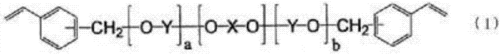
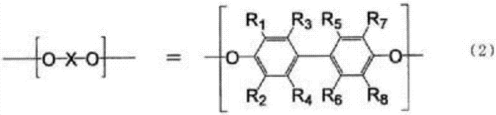
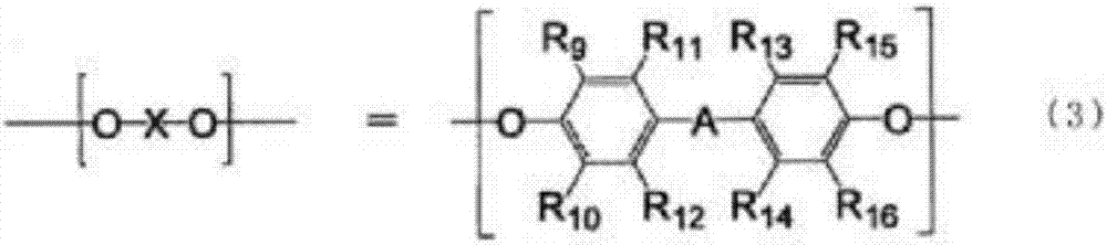
[0140] OPE2200: oligophenylene ether (modified polyphenylen...

Embodiment 1

[0174] In Examples 1 to 14, the high-frequency electrical characteristics (dielectric constant (ε), dielectric loss factor (tanδ)) and peel strength were all good. The differences of Examples 2 to 10 with respect to Example 1 are as follows.

Embodiment 2

[0175] Example 2: Combination use of component (B-1) and component (B-2).


PUM

PropertyMeasurementUnit
particle diameteraaaaaaaaaa
particle sizeaaaaaaaaaa

Abstract

Provided are: an insulating film having excellent adhesive strength to metal foil that forms FPC wiring and to FPC substrate material such as polyimide film and exhibiting electrical characteristics in the high frequency range, specifically, low dielectric constant (epsilon) and low dielectric tangent (tan delta) in the 1-10 GHz frequency range; and a resin composition used in manufacturing said insulating film. This resin composition contains (A) a thermosetting resin having styrene groups on the ends and having a phenylene ether backbone, (B) a hydrogenated styrene thermoplastic elastomer, and (C) a polytetrafluoroethylene filler, and contains 40 mass% to 80 mass% of the component (C) with respect to the total mass of the components (A)-(C).

Description

technical field [0001] The present invention relates to a resin composition, an insulating film using the resin composition, and a semiconductor device. Background technique [0002] In recent years, due to the development of miniaturization, light weight and high performance of equipment, printed wiring boards used in electrical and electronic equipment, especially multilayer printed wiring boards, require further high multilayer and high density , Thinning, lightweight, high reliability and formability, etc. [0003] Moreover, along with the demand for the speed-up of the transmission signal of the recent printed wiring board, the high-frequency increase of a transmission signal progresses remarkably. Therefore, materials used for printed wiring boards are required to be able to reduce the loss of electrical signals in a high-frequency region, specifically, a region with a frequency of 1 GHz or higher. [0004] Patent Document 1 discloses a method of manufacturing a fluo...

Claims


Application Information

Patent Timeline
Patent Type & Authority Applications(China)
IPC IPC(8): C08L27/18C08K5/548C08L25/04C08L71/12H05K1/03H05K3/28
CPCC08K5/548C08L25/04C08L27/18C08L71/12H05K1/03H05K3/28H05K1/0353
Inventor 小松史和吉田真树寺木慎
Owner NAMICS CORPORATION
Why Eureka
Try Eureka